Beam splitting laser cutting method for silicon-based wafer

A laser cutting, silicon-based crystal technology, used in laser welding equipment, welding equipment, metal processing equipment, etc., to enhance mobility, reduce risks, and improve cutting quality.

Active Publication Date: 2019-02-19
SHENZHEN STS MICROELECTRONICS
View PDF10 Cites 5 Cited by
  • Summary
  • Abstract
  • Description
  • Claims
  • Application Information

AI Technical Summary

Problems solved by technology

However, the patent document TWI628027B has no step-by-step cutting technology scheme using multi-beam array laser knives with different pattern shapes.

Method used


Image

  • Beam splitting laser cutting method for silicon-based wafer
  • Beam splitting laser cutting method for silicon-based wafer
  • Beam splitting laser cutting method for silicon-based wafer

Examples


Embodiment Construction

[0045] In the following, the present invention will be further described with reference to the drawings and specific implementations.

[0046] First, the conceptual design of the present invention is described as follows:

[0047] 1. Introduction to cutting process

[0048] Filming steps:

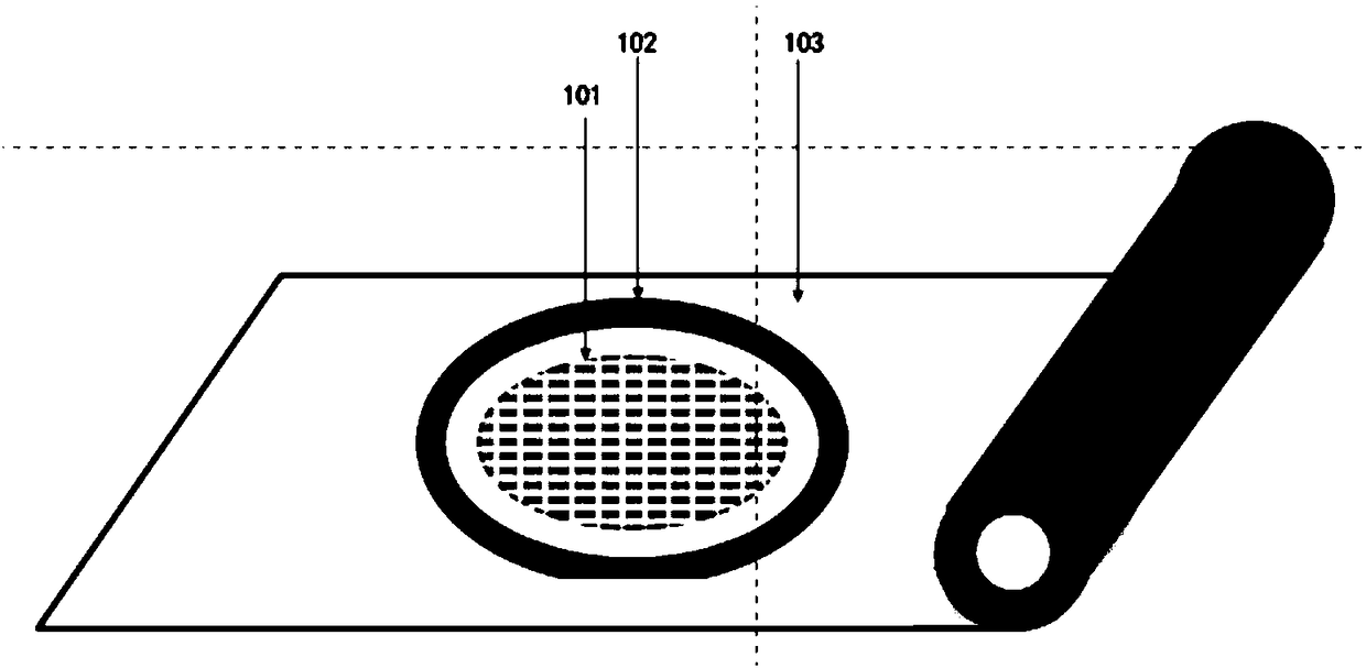
[0049] Such as figure 1 As shown, the silicon-based wafer 101 and the iron ring 102 are attached to the film 103, and the film part outside the iron ring 102 is scratched with a blade, and the film part inside the iron ring 102 is retained.

[0050] Purpose: Attach the silicon-based wafer 101 to the film 103 and fix it with the iron ring 102 to facilitate processing, cutting, and patching.

[0051] Cutting steps:

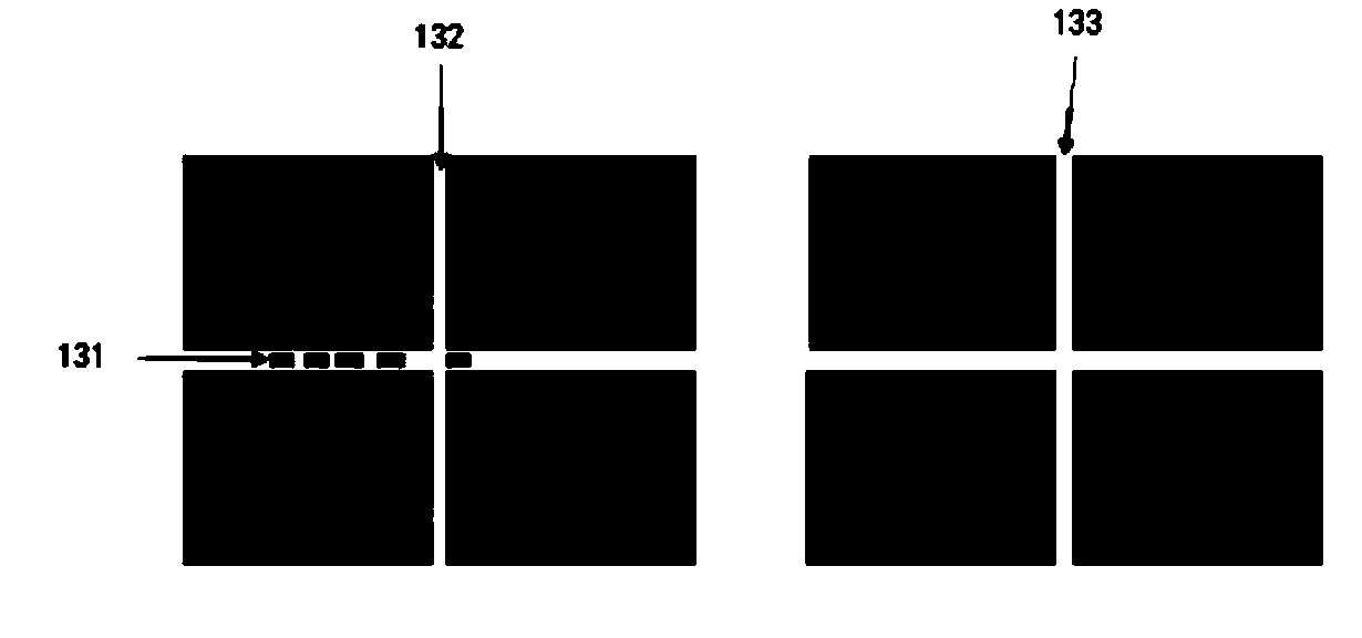
[0052] Such as figure 2 As shown, the wafer is cut once or multiple times in a certain cutting manner according to a certain cutting mode, such as depth, speed, position, and width.

[0053] Purpose: Divide the entire wafer into independent, functional chips 10.

[0054] UV irradiation ste...


PUM


Abstract

The invention discloses a beam splitting laser cutting method for a silicon-based wafer. The beam splitting laser cutting method for the silicon-based wafer is used for cutting the silicon-based waferinto independent chips, and is characterized by comprising the following steps of a pretreatment step; a diffraction light splitting step, wherein a single beam laser (105) is split into a pluralityof beams of laser (108) through a grating device (106) and a light beam pattern is formed; a beam splitting cutting step, wherein a laser cutter of the style is used for cutting the silicon-based wafer; and a postprocessing step. The beam splitting laser cutting method for the silicon-based wafer achieves the technical effects that the wafer cutting speed is increased, and meanwhile the cutting quality of the wafer is improved.

Description

Technical field [0001] The present invention relates to the technical field of cutting with laser beams, in which the beam is divided into multiple beams (B23K26 / 067), and a mask is used to form the pattern shape of the laser beam (B23K 26 / 06). The present invention particularly relates to silicon-based crystals. Circular beam splitting laser cutting method. Background technique [0002] Smart devices have developed rapidly in recent years, and people's requirements for smart devices are also developing in the direction of multi-function, precision, and high integration. And this kind of demand also puts forward the small, thin, light process requirements and the performance requirements of ultra-low energy consumption, fast heat dissipation, and high amplification efficiency for electronic components. [0003] Due to the impact of small, thin, and lightweight chips, the traditional wafer blade cutting process has gradually shown a decline in chip cutting speed and reliability, an...

Claims


Application Information

Patent Timeline
Patent Type & Authority Applications(China)
IPC IPC(8): B23K26/38B23K26/402B23K26/067B23K26/02B23K26/70
CPCB23K26/02B23K26/0673B23K26/38B23K26/402B23K26/70
Inventor 詹苏庚吴迪彭立和王红丁锋
Owner SHENZHEN STS MICROELECTRONICS
Why Eureka
Try Eureka