Technology for increasing capacity of silicon-based heterojunction solar cells

A solar cell and heterojunction technology, applied in circuits, photovoltaic power generation, electrical components, etc., can solve the problems of affecting the temperature environment, easily damaged heating components, unstable heating environment, etc., to save equipment costs, improve equipment productivity, The effect of saving processing time

Active Publication Date: 2014-11-19
IDEAL ENERGY (SHANGHAI) SUNFLOWER THIN FILM EQUIPMENT LTD
View PDF8 Cites 3 Cited by
  • Summary
  • Abstract
  • Description
  • Claims
  • Application Information

AI Technical Summary

Problems solved by technology

However, since the feeding chamber is often exposed to the atmosphere, heating here will cause some residual oxygen, water vapor and other substances to exist in the chamber, and these substances are likely to react on the surface of the silicon wafer at high temperature, affecting the passivation of the heterojunction interface. effect, which affects the efficiency of solar cells
On the other hand, when the film feeding chamber is connected to the atmosphere, the heat will be continuously transferred from the outside to the film feeding chamber, affecting its temperature environment, resulting in unstable heating environment, affecting the production yield of products and making the heating parts easy to damage

Method used


Image

  • Technology for increasing capacity of silicon-based heterojunction solar cells
  • Technology for increasing capacity of silicon-based heterojunction solar cells
  • Technology for increasing capacity of silicon-based heterojunction solar cells

Examples


no. 1 example

[0053] The invention provides a process for increasing the production capacity of a silicon-based heterojunction solar cell, which is used to prepare a silicon-based thin film in the silicon-based heterojunction solar cell, image 3 A schematic flow diagram of the first embodiment is shown, the process includes the following steps:

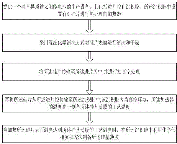
[0054] Step S1, providing production equipment for silicon-based heterojunction solar cells, which includes a wafer feeding chamber and a deposition chamber, and the deposition chamber is provided with a heater for heat-treating silicon wafers;

[0055] Step S2, cleaning and drying the surface of the silicon wafer by means of wet chemical cleaning;

[0056] Step S3, transferring the silicon wafer into the wafer feeding chamber, and performing vacuuming treatment;

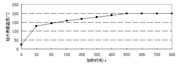
[0057] In step S4, the silicon wafer is transferred from the feeding chamber to the deposition chamber, the deposition chamber is in a vacuum environment, and the temperature of the he...

no. 2 example

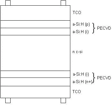
[0080]In view of the industrial need to deposit different types of multi-layer amorphous silicon films on the surface of silicon-based heterojunction solar cells, such as depositing intrinsic amorphous silicon films, P-type amorphous silicon films, and N-type amorphous silicon films on silicon wafers Crystalline silicon thin film, the present invention also provides a process for increasing the production capacity of silicon-based heterojunction solar cells, which is used to prepare intrinsic amorphous silicon thin films and doped amorphous silicon films in the silicon-based heterojunction solar cells Silicon film, Figure 5 It is a schematic flow chart of the process for increasing the production capacity of silicon-based heterojunction solar cells in the second embodiment of the present invention. The process includes the following steps:

[0081] Step S1, providing production equipment for silicon-based heterojunction solar cells, which includes a wafer feeding chamber and...


PUM


Abstract

The invention relates to a technology for increasing the capacity of silicon-based heterojunction solar cells. The technology comprises the steps that a production device, which comprises a wafer inlet chamber and a deposition chamber, of the silicon-based heterojunction solar cells is provided, and the deposition chamber is internally provided with a heater which implements heat treatment on silicon wafers; the surfaces of the silicon wafers are cleaned and dried in a wet chemical cleaning method; the silicon wafers are transmitted to the wafer inlet chamber, and vacuumizing is carried out; the silicon wafers are transmitted from the wafer inlet chamber to the deposition chamber, the internal of the deposition chamber includes a vacuum environment, and the preset temperature of the heater is greater than the technical temperature for preparing silicon-based films; and when the surface temperature of the silicon wafers is increased to the technical temperature of the silicon-based films due to heating, the silicon-based films are prepared in a chemical vapor deposition method in the deposition chamber. The technology can improve the equipment capacity and reduce the production cost while ensuring the quality of films.

Description

[0001] technical field [0002] The invention relates to the field of silicon-based heterojunction solar cells and the field of semiconductor manufacturing, in particular to a process capable of increasing the production capacity of silicon-based heterojunction solar cells. technical background [0003] At present, the common preparation of single-sided or double-sided silicon-based heterojunction solar cells requires the deposition of silicon-based or carbon-based films on silicon wafers, such as amorphous silicon films, microcrystalline silicon films, nano-silicon films, silicon oxide films, carbonized Silicon film, silicon nitride film, etc. These thin film preparation processes all include the following two steps: first, heat the silicon wafer to the process temperature (130-350°C) in vacuum, and then deposit a very thin film layer (2-20nm) on the surface of the silicon wafer under the process temperature condition . At present, people usually use two ways to complete ...

Claims


Application Information

Patent Timeline
Patent Type & Authority Applications(China)
IPC IPC(8): H01L21/67H01L21/205
CPCH01L21/2053H01L21/67103H01L21/67109H01L31/202Y02E10/50
Inventor 陈金元汪训忠其他发明人请求不公开姓名
Owner IDEAL ENERGY (SHANGHAI) SUNFLOWER THIN FILM EQUIPMENT LTD
Why Eureka
Try Eureka