Method for preventing gold plating lateral erosion and gold finger copper exposure of printed circuit boards

A printed circuit board and circuit board technology, applied in the directions of printed circuit, printed circuit manufacturing, printed circuit secondary processing, etc., can solve the problems of exposed copper on gold fingers, inability to apply gold on gold fingers, and increased cost of printed circuit boards. The effect of preventing gold-plated side corrosion and preventing gold fingers from exposing copper

Inactive Publication Date: 2019-02-19
JIANDING HUBEI ELECTRONICS CO LTD
View PDF3 Cites 0 Cited by
  • Summary
  • Abstract
  • Description
  • Claims
  • Application Information

AI Technical Summary

Problems solved by technology

[0006] (2) Solder resist first, and then gold plating, because the ink is not developed cleanly or the ink is anti-sticky, it will cause the gold fingers to be unable to be gold-plated, resulting in exposed copper on the gold fingers
[0007] In response to the above-mentioned deficiencies, the general practice of the industry is to repair the gold-plated side etching and gold finger exposed copper. Although the gold-plated side etching and gold finger exposed copper can be improved, it requires additional labor and leads to an increase in the cost of printed circuit boards.
[0008] In addition, although the above-mentioned repairing method can improve the gold-plated undercut and the exposed copper of the gold finger, there are still defects due to imperfect repairing, resulting in a high failure rate of the printed circuit board

Method used


Image

  • Method for preventing gold plating lateral erosion and gold finger copper exposure of printed circuit boards

Examples


Embodiment

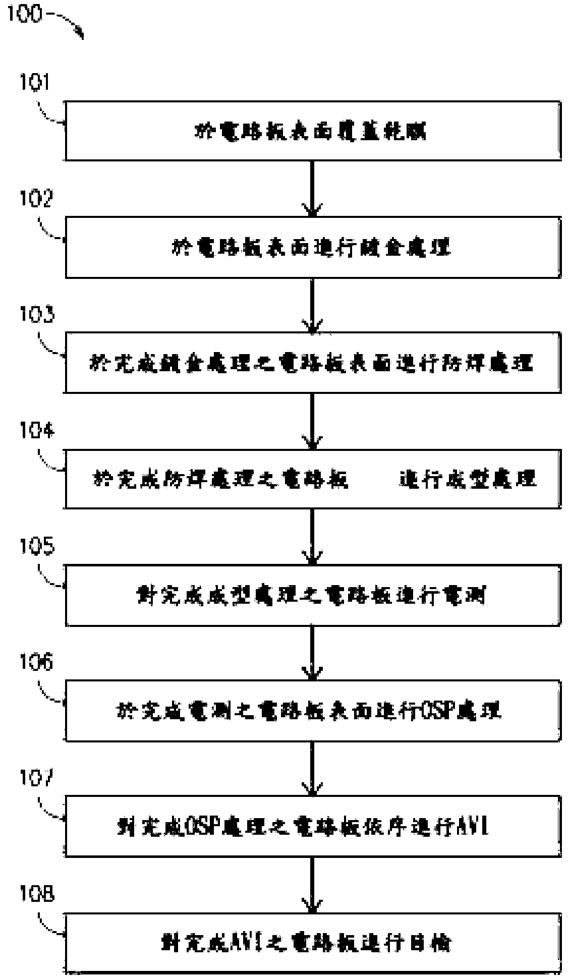
[0039] see figure 1 As shown, a method flow 100 for preventing underside corrosion of gold-plated printed circuit boards and exposed copper on gold fingers provided by the present invention includes the following steps:

[0040] Step 101: Cover the surface of the circuit board with a dry film; cover the dry film where no gold plating is required;

[0041] Step 102: performing gold plating on the surface of the circuit board;

[0042] Step 103: Solder resist treatment is performed on the surface of the gold-plated circuit board; the solder resist treatment is to use ink to protect parts that do not need to be soldered.

[0043] Step 104: Carry out molding treatment on the circuit board that has completed the solder mask treatment, and make it into the size required by the customer;

[0044] Step 105: Conduct electrical testing on the circuit board that has completed the molding process;

[0045] Step 106: Perform OSP (Organic Solderability Preservative, Organic Solderability...


PUM


Abstract

The invention relates to a process for printed circuit boards, belongs to the technical field of printed circuit boards, and particularly relates to a method for preventing gold plating lateral erosion and gold finger copper exposure of printed circuit boards. The method has the advantages that gold plating treatment is carried out on the surfaces of circuit boards at first, then solder mask treatment is carried out on the surfaces, which are already subjected to gold plating treatment, of the circuit boards, accordingly, solder mask attachment effects can be prevented from being affected by the length of the soaking time of gold tanks and fluctuation of currents of the gold tanks in gold plating procedures, and gold finger root lateral erosion can be prevented; the problems of incapability of coating gold on gold fingers and gold finger copper exposure during gold plating due to the fact that printing ink is not thoroughly developed or is reversely adhered can be solved; gold platinglateral erosion and gold finger copper exposure of the printed circuit boards truly can be prevented by the aid of the method.

Description

technical field [0001] The invention relates to a printed circuit board process, which belongs to the technical field of printed circuit boards, and in particular relates to a method for preventing the gold-plated side erosion of the printed circuit board and the exposed copper of gold fingers. Background technique [0002] With the rapid improvement of industrial development capabilities in various countries around the world, the consumer market is getting bigger and bigger, and printed circuit board (PCB) companies are growing rapidly. [0003] The known manufacturing process of a printed circuit board mainly includes the following steps: performing solder resist treatment on the surface of the printed circuit board, then pasting a dry film, and then performing gold plating. [0004] Since the anti-soldering treatment is to use ink to protect the parts that do not need to be welded, the lack of the above-mentioned conventional methods mainly includes: [0005] (1) Solder ...

Claims


Application Information

Patent Timeline
Patent Type & Authority Applications(China)
IPC IPC(8): H05K3/28
CPCH05K3/282H05K2203/162
Inventor 費云祥高心法雷成周翠翠陳志堅
Owner JIANDING HUBEI ELECTRONICS CO LTD
Why Eureka
Try Eureka