Silicon-based tunable laser

A tunable laser, silicon-based technology, used in lasers, laser parts, semiconductor lasers, etc., can solve the problems of slow progress of core device lasers, complex tunable laser fabrication, and hinder laser on-chip integration, achieving low loss and simple structure. , Improve the effect of wavelength stability

Active Publication Date: 2019-02-22
WUHAN POST & TELECOMM RES INST CO LTD +1
View PDF11 Cites 12 Cited by
  • Summary
  • Abstract
  • Description
  • Claims
  • Application Information

AI Technical Summary

Problems solved by technology

However, the research on core device lasers has been slow, mainly because silicon materials are indirect bandgap semiconductors with low luminous efficiency, and can only use III-V materials as gain media; in addition, the mode spots of traditional lasers and CMOS process silicon waveguides Mismatch also hampers on-chip integration of lasers
[0004] At present, tunable lasers are the main light source in the field of coherent optical communication. Traditional tunable lasers are complicated to manufacture and cost high.

Method used


Image

  • Silicon-based tunable laser

Examples


Embodiment Construction

[0022] The following will clearly and completely describe the technical solutions in the embodiments of the present application with reference to the drawings in the embodiments of the present application. Obviously, the described embodiments are part of the embodiments of the present application, not all of them.

[0023] In this application, when it is described that a specific component is located between a first component and a second component, there may or may not be an intermediate component between the specific component and the first component or the second component; When a specific component is connected to other components, the specific component may be directly connected to the other component without an intermediate component, or may not be directly connected to the other component but has an intermediate component.

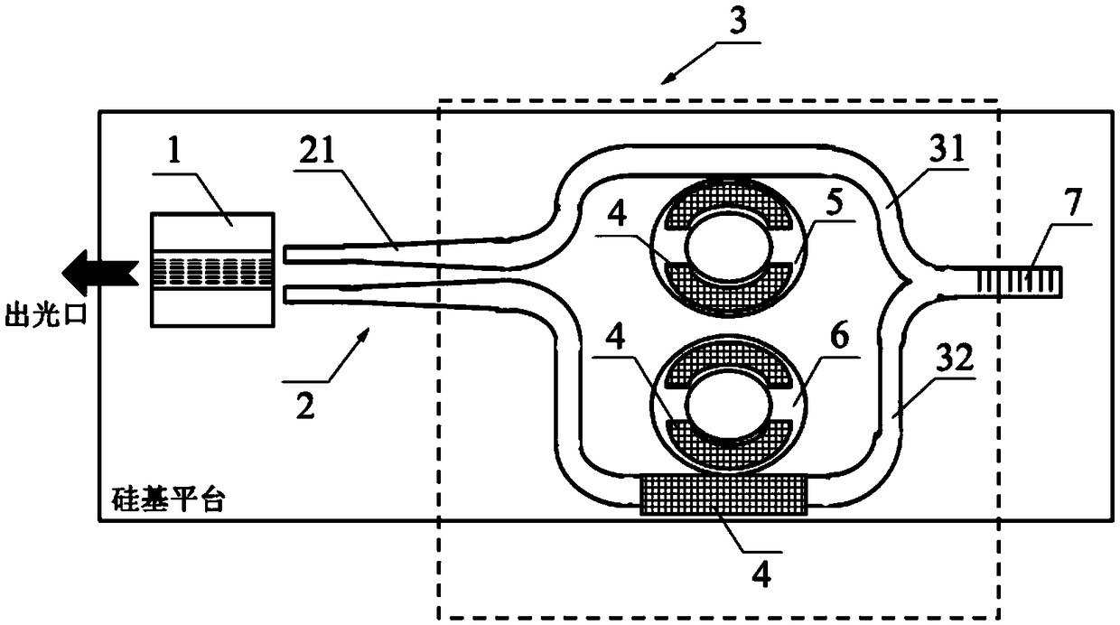
[0024] see figure 1 as shown, figure 1 is a layout diagram of a silicon-based tunable laser, which includes a semiconductor amplifier 1, a mode sp...


PUM


Abstract

The invention discloses a silicon-based tunable laser, and relates to the field of silicon-based photonics and integrated optoelectronics. The silicon-based tunable laser includes a semiconductor amplifier integrated on a silicon-based platform, a spot-size converter which is connected to a backlight end of the semiconductor amplifier and includes a double inverted cone waveguide, an asymmetric Mach-Zehnder interferometer (AMZI) which includes a first arm and a second arm of unequal length, wherein input ends of the first arm and the second arm are cascaded with the double inverted cone waveguide, output ends of the first arm and the second arm intersect to form a single waveguide and a heater is arranged on the second arm, a first micro-ring filter which is cascaded with the first arm andprovided with heaters, a second micro-ring filter which is cascaded with the second arm and provided with heaters, and a distributed Bragg reflector (DBR) which is used for realizing optical feedbackand formed on the single waveguide. The silicon-based tunable laser has the advantages of low manufacturing cost, simple process and high integration, benefits large-scale production, and can improvetuning bandwidth and wavelength stability.

Description

technical field [0001] The invention relates to the field of silicon-based photonics and integrated optoelectronics, in particular to a silicon-based tunable laser. Background technique [0002] With the development of information technology and CMOS (Complementary Metal Oxide Semiconductor, Complementary Metal Oxide Semiconductor) process technology, people require faster and faster computing speed of the system and smaller and smaller chip sizes. However, the silicon integrated circuit based on the traditional etching process has already reached the technological limit of the chip; mainly because of the continuous shrinking of the size, the interconnection delay effect and energy consumption of the traditional electrical interconnection-based integrated circuit gradually appear. This limits the improvement of the system's operating speed and integration. Compared with the electrical interconnection technology, the optical interconnection technology using photonics as the ...

Claims


Application Information

Patent Timeline
Patent Type & Authority Applications(China)
IPC IPC(8): H01S5/065H01S5/10H01S5/125H01S5/022
CPCH01S5/0651H01S5/1042H01S5/125H01S5/0237
Inventor 冯朋肖希王磊李淼峰张宇光胡晓陈代高
Owner WUHAN POST & TELECOMM RES INST CO LTD
Why Eureka
Try Eureka