Method for uniformizing temperature field of current assisted sintered nano-silver soldering paste on basis of DBC (Direct Bonded Copper) ceramic substrate

A uniform current and auxiliary sintering technology, which is applied in the direction of circuits, electrical components, and electrical solid devices, can solve problems such as poor reliability of fatigue resistance, low mechanical strength, and uneven temperature distribution, so as to achieve uniform distribution, prolong service life, Effect of improving mechanical strength and fatigue resistance reliability

Active Publication Date: 2019-03-01
TIANJIN UNIV
View PDF5 Cites 2 Cited by
  • Summary
  • Abstract
  • Description
  • Claims
  • Application Information

AI Technical Summary

Problems solved by technology

[0006] The present invention mainly solves the problem of uneven temperature distribution in the process of current-assisted rapid sintering nano-silver solder paste connecting IGBT chips and diode chips and DBC substrates, and the resulting low mechanical strength and poor fatigue resistance of the sintered joints. The study found that the shape of the electrode significantly affects the temperature distribution of the nano-silver solder paste during the current-assisted rapid sintering process. By designing the special-shaped electrode and position distribution of the applied current, the temperature field of the current-assisted sintered nano-silver solder paste is evenly distributed, and the overall mechanical strength of the sintered joint is improved. and fatigue reliability

Method used


Image

  • Method for uniformizing temperature field of current assisted sintered nano-silver soldering paste on basis of DBC (Direct Bonded Copper) ceramic substrate
  • Method for uniformizing temperature field of current assisted sintered nano-silver soldering paste on basis of DBC (Direct Bonded Copper) ceramic substrate
  • Method for uniformizing temperature field of current assisted sintered nano-silver soldering paste on basis of DBC (Direct Bonded Copper) ceramic substrate

Examples


Embodiment Construction

[0028] Below in conjunction with the accompanying drawings, a detailed description will be given of specific implementations based on the uniform current assisted sintering of nano-silver solder paste temperature field on copper-clad ceramic substrates and the rapid sintering connection of IGBT chips / diode chips and copper-clad ceramic substrates (DBC) substrates.

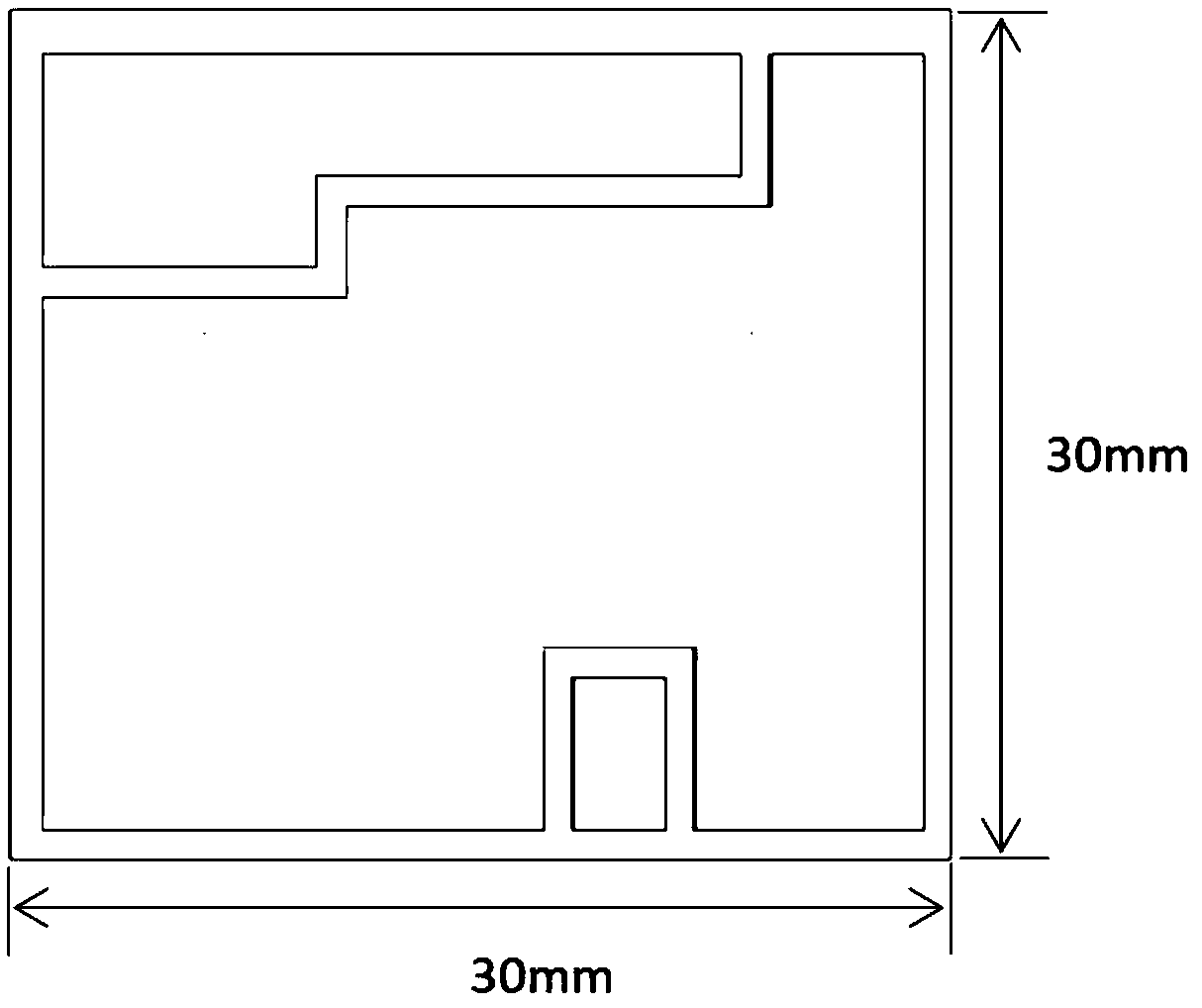
[0029] (1) Before the experiment, place the copper-clad ceramic substrate, chips, and rubber rods in a beaker filled with absolute ethanol, then put them into an ultrasonic cleaner for oscillating cleaning for 10 minutes, and wipe them with dust-free paper after taking them out. The copper-clad ceramic substrate used in the present invention is as figure 1 As shown, the size is 30mm×30mm.

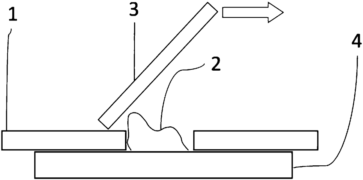
[0030] (2) Printing nano-silver solder paste: according to the chip size, paste four 50μm-90μm thick high-temperature-resistant Kapton tape 1 on the surface of the DBC substrate, and the enclosed area is slightly larger than the...


PUM


Abstract

The invention relates to a method for uniformizing a temperature field of current assisted sintered nano-silver soldering paste on the basis of a DBC (Direct Bonded Copper) substrate. The shape of a copper layer of the DBC substrate and a region where an electrode pressure head after the nano-silver soldering paste is printed can be placed are combined; each special-shaped electrode is of a rightangle L shape; an interior angle of each special-shaped electrode is in transition of one fourth of an arc; before sintering, the electrodes are pre-pressed at both ends of the DBC substrate; appliedpulse direct currents uniformly flow the soldering paste; the sintering temperature field of the nano-silver soldering paste is uniformly distributed; and a chip is uniformly heated. According to theinvention, a problem of uneven temperature in process of rapidly sintering the nano-silver soldering paste by the currents is successfully solved; by designing the special-shaped electrodes applying the currents and position distribution, uniform distribution of the temperature field in the nano-silver soldering paste pulse current assisted sintering process and one-time rapid sintering connectionbetween a sintered nano-silver soldering paste IGBT chip/diode chip and the DBC ceramic substrate are implemented; obtained compactness reaches over 90%; mechanical intensity and anti-fatigue reliability of a sintering interconnection layer are greatly improved; and the service life is prolonged.

Description

technical field [0001] The invention relates to a method for assisting the temperature field of sintering nano-silver solder paste based on a uniform current of a copper-clad ceramic substrate, which belongs to the field of packaging of electronic components. Background technique [0002] DBC (Direct Bonded Copper) copper-clad ceramic substrate has excellent thermal conductivity, high insulation, high bonding strength, easy to print graphics, good solderability, etc., and has been widely used in power electronics such as GTR, IGBT, MCT, etc. module. In module manufacturing, the limited space of the DBC substrate is divided into three mutually insulated areas: the chip welding area, the electrode terminal welding area, and the bonding wire area. The chip bonding area occupies the main area of ​​the DBC, and enough space must be left for chip bonding in the design. [0003] Nano-silver solder paste has the advantages of high melting point (961°C), excellent electrical and th...

Claims


Application Information

Patent Timeline
Patent Type & Authority Applications(China)
IPC IPC(8): H01L21/60H01L25/00
CPCH01L24/83H01L25/50H01L2224/83095H01L2224/8384
Inventor 梅云辉张心印李欣陆国权
Owner TIANJIN UNIV
Why Eureka
Try Eureka