

A method for testing electrical parameters of storage media and wafer-level integrated circuits
A technology of electrical parameters and integrated circuits, applied in the direction of circuits, semiconductor/solid-state device testing/measurement, electrical components, etc., can solve the problem of improving test efficiency without substantial contribution, unable to meet the urgent needs of high-speed measurement, and unavoidable unified testing Structural testing and other issues to achieve the effect of improving test efficiency, shortening test time, and improving service life
- Summary
- Abstract
- Description
- Claims
- Application Information
AI Technical Summary
Problems solved by technology
Method used
Image

Examples
Embodiment 1
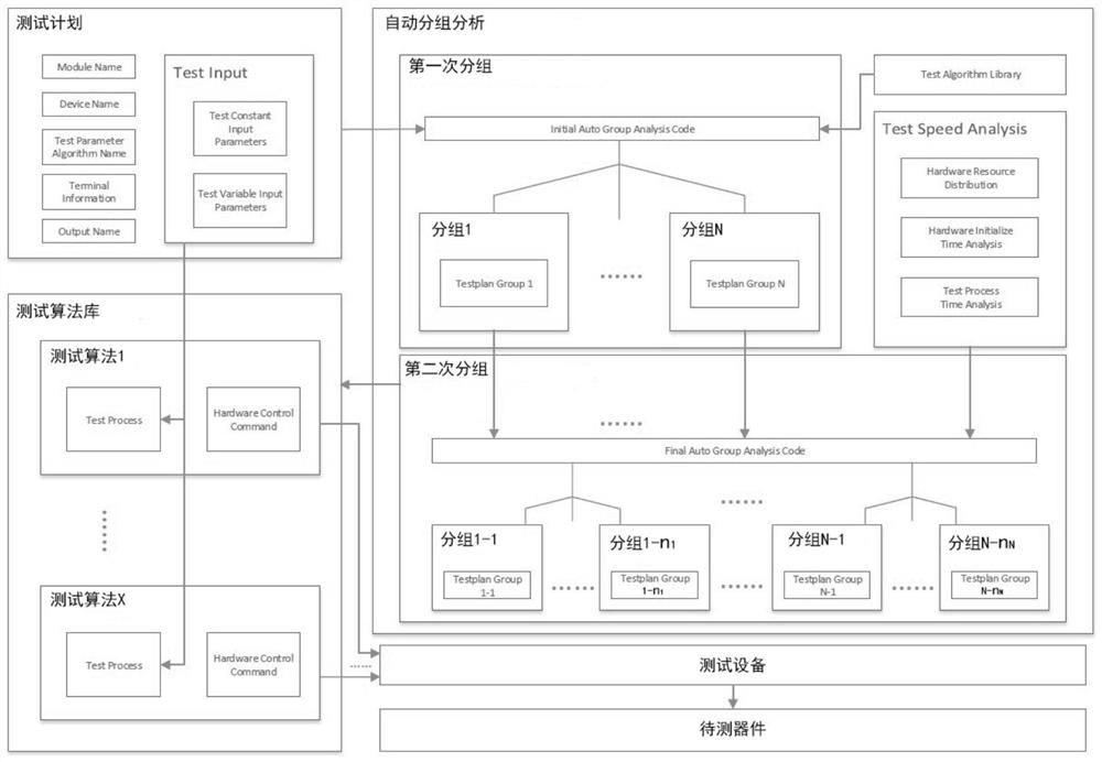
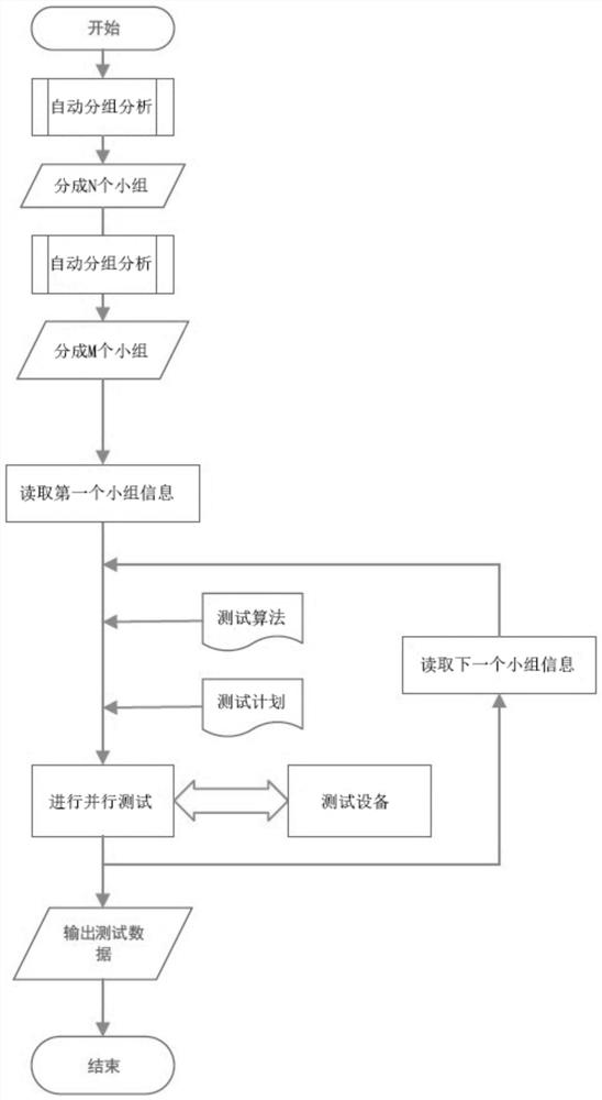
[0059] like figure 2 As shown, this embodiment provides a method for testing electrical parameters of a wafer-level integrated circuit, the method comprising the following steps:
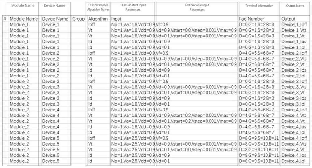
[0060] a) Divide the test plan group according to the electrical parameters of the structure to be tested and the test input parameters required for the test; wherein, for the specific content of the test plan, refer to image 3 . In order to further illustrate the technical solution of the present embodiment, the above-mentioned process is described in detail: the range during the test Ids is 1e -3 A, the protection current is 1e -3 A, The test with the working voltage of the addressing circuit at 1.8V is divided into one group. If there are different configuration parameters, they need to be grouped into another group. The measurement of all test structures in a group only needs to configure the test input parameters once. For the current high-integration chips, it avoids the time to repeated...
PUM
 Abstract
Description
Claims
Application Information