Transverse high-voltage device with low specific on-resistance

A specific on-resistance, lateral high voltage technology, applied in semiconductor devices, electrical components, circuits, etc., can solve the problems of increased device on-resistance, low specific on-resistance, etc., and achieve reduced on-resistance and good compatibility , Optimizing the effect of surface electric field distribution

Inactive Publication Date: 2019-03-01
UNIV OF ELECTRONICS SCI & TECH OF CHINA
View PDF5 Cites 0 Cited by
  • Summary
  • Abstract
  • Description
  • Claims
  • Application Information

AI Technical Summary

Problems solved by technology

[0003] The invention aims at the problem that the on-resistance of the device increases due to the use of the drift region with low doping concentration in order to obtain a high withstand voltage in the traditional lateral high-voltage power device, and proposes a lateral high-voltage device with a low specific on-resistance

Method used


Image

  • Transverse high-voltage device with low specific on-resistance
  • Transverse high-voltage device with low specific on-resistance
  • Transverse high-voltage device with low specific on-resistance

Examples


Embodiment 1

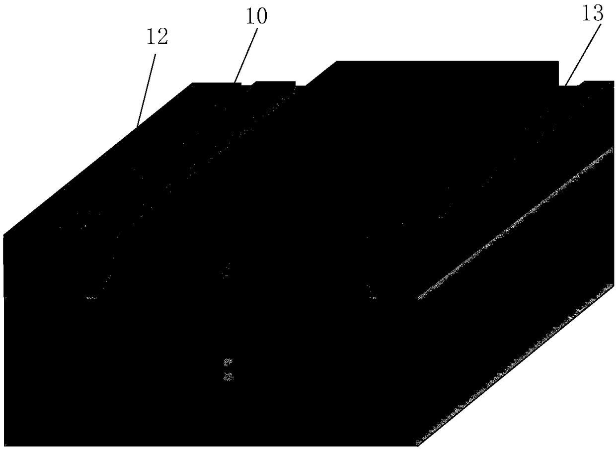
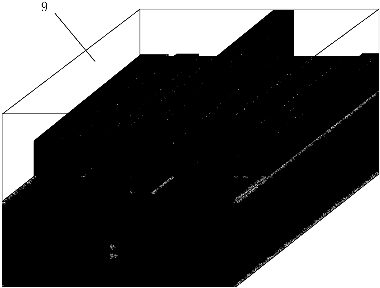
[0027] Such as figure 2 , image 3 As shown, this embodiment focuses on one electrode, and n electrodes 11 are actually provided, where n≥2. The lateral high-voltage device with low specific on-resistance in this embodiment includes a second-type impurity-doped semiconductor substrate 1; The first type doped impurity drift region 3 and the second type doped impurity well region 4 formed on the second type doped impurity semiconductor substrate 1; formed in the second type doped impurity well region 4 The second type doped impurity contact region 5 and the first type doped impurity source region 6; the first type doped impurity well region 7 formed in the first type doped impurity drift region 3; forming The first-type doped impurity drain region 8 in the first-type doped impurity well region 7; formed above and on the left and right sides of the first-type doped impurity drift region 3 and the second-type doped impurity well region 4 The first dielectric layer 9 on the side...

Embodiment 2

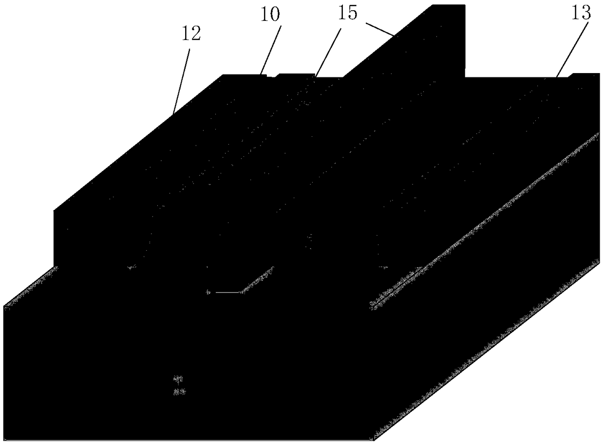
[0029] Such as Figure 4 As shown, there are two electrodes in this embodiment. The difference between this embodiment and Embodiment 1 is that the dielectric layer 15 uses a low-k dielectric, and the thickness of the dielectric 15 decreases in proportion to the vacuum dielectric constant, reducing the use area.

Embodiment 3

[0031] Such as Figure 5As shown, there are five electrodes in this embodiment, and the difference between this embodiment and Embodiment 1 is: among any two adjacent electrodes among the five electrodes 11, one end close to the first type doped impurity well region 7 The distance W between the inner surface of the electrode and the outer surface of the first type doped impurity drift region 3 i+1 , not less than the distance W between the inner surface of the electrode near one end of the second-type doped impurity well region 4 and the outer surface of the first-type doped impurity drift region 3 i , the distance H between the lower surface of the electrode near one end of the first type doped impurity well region 7 and the upper surface of the first type doped impurity drift region 3 i+1 , not less than the distance H between the lower surface of the electrode near one end of the second-type doped impurity well region 4 and the upper surface of the first-type doped impurit...


PUM


Abstract

The invention provides a transverse high-voltage device with low specific on-resistance. The transverse high-voltage device with low specific on-resistance comprises a second-type doping impurity semiconductor substrate, a first-type doping impurity drift region, a second-type doping impurity well region, a second-type doping impurity contact region, a first-type doping impurity source region, a first-type doping impurity well region, a first-type doping impurity drain region, dielectric layers, a poly-silicon gate, source metal and drain metal, wherein n electrodes are arranged right above aregion between the second-type doping impurity well region and the first-type doping impurity well region and in the dielectric layers at a left side and a right side, n is more than or equal to 2, aninterval is kept between projections of two arbitrary electrodes in the n electrodes in a direction from the second-type doping impurity well region to the first-type doping impurity well region, andeach electrode is biased to fix different potentials. With the transverse high-voltage device provided by the invention, the voltage resistance of the device can be improved, meanwhile, the on-resistance of the device is reduced, and the conflict between the on-resistance and the voltage resistance of the transverse high-voltage device is effectively reduced.

Description

technical field [0001] The invention belongs to the field of semiconductor power devices, in particular to a lateral high-voltage device with low specific on-resistance. Background technique [0002] Lateral high-voltage devices are an essential part of the development of high-voltage power integrated circuits. They have the advantages of high withstand voltage, high input impedance, good safe working area, and low power consumption. They have been widely used in motor drives, automotive electronics, and industrial control. in the power switching device. When the lateral high-voltage device works in a high withstand voltage environment, it needs to adopt a long drift region, so the lateral high-voltage device will be accompanied by high on-resistance, resulting in higher power consumption of the device during normal operation. In practical applications, it is necessary to reduce the on-resistance of the device as much as possible while ensuring the withstand voltage of the ...

Claims


Application Information

Patent Timeline
Patent Type & Authority Applications(China)
IPC IPC(8): H01L29/78H01L29/739H01L29/40H01L29/06
CPCH01L29/0684H01L29/404H01L29/407H01L29/7393H01L29/7394H01L29/7823H01L29/7824
Inventor 周锌赵凯马阔王睿迪乔明张波
Owner UNIV OF ELECTRONICS SCI & TECH OF CHINA
Why Eureka
Try Eureka