Quantum dot light-emitting layer raw material preparation method and light-emitting device applying method

A quantum dot light-emitting and light-emitting device technology, which is applied in the direction of electric solid-state devices, semiconductor devices, organic semiconductor devices, etc., can solve the consistency problems such as not fully considering the phase structure, increase the difficulty of large-scale production process, and the advantages are not obvious. and other issues, to achieve the effect of increasing charge transport performance, increasing charge transport, and reducing leakage current

Inactive Publication Date: 2019-03-01
嘉兴纳鼎光电科技有限公司
View PDF5 Cites 3 Cited by
  • Summary
  • Abstract
  • Description
  • Claims
  • Application Information

AI Technical Summary

Problems solved by technology

This method requires precise control of the thickness of the insulating layer, which increases the difficulty of mass production;
[0006] 2. Replace the traditional organic hole transport layer with inorganic oxides such as NiO to increase the efficiency of hole injection, but the advantages of this method have not been clearly reflected so far;
Although the material of the transport layer is consistent with the shell material of the quantum dot light-emitting layer, this method does not fully consider the contradiction between the surface ligands and the orthogonal solvent selection of the two, as well as the consistency of the phase structure; at the same time, the sol-gel Processes such as chemical baths or chemical baths may cause damage to the existing functional layer, which also increases the complexity of the process

Method used


Image

  • Quantum dot light-emitting layer raw material preparation method and light-emitting device applying method
  • Quantum dot light-emitting layer raw material preparation method and light-emitting device applying method
  • Quantum dot light-emitting layer raw material preparation method and light-emitting device applying method

Examples


Embodiment 1

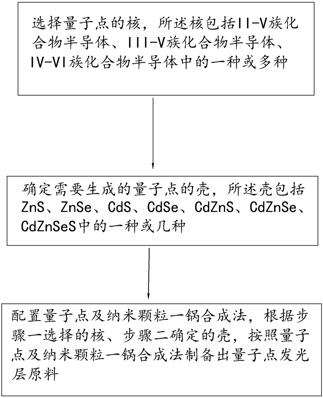
[0032] Embodiment 1, the preparation method of quantum dot light-emitting layer raw materials, referring to the figure, includes:

[0033] Step 1, selecting the nucleus of the quantum dot, which includes one or more of II-V compound semiconductors, III-V compound semiconductors, and IV-VI compound semiconductors;

[0034] Step 2, determining the shell of the quantum dot that needs to be generated, the shell includes one or more of ZnS, ZnSe, CdS, CdSe, CdZnS, CdZnSe, and CdZnSeS;

[0035] Step 3, configure the quantum dots and nanoparticles one-pot synthesis method, and prepare the quantum dot light-emitting layer raw material according to the quantum dots and nanoparticles one-pot synthesis method according to the core selected in step 1 and the shell determined in step 2.

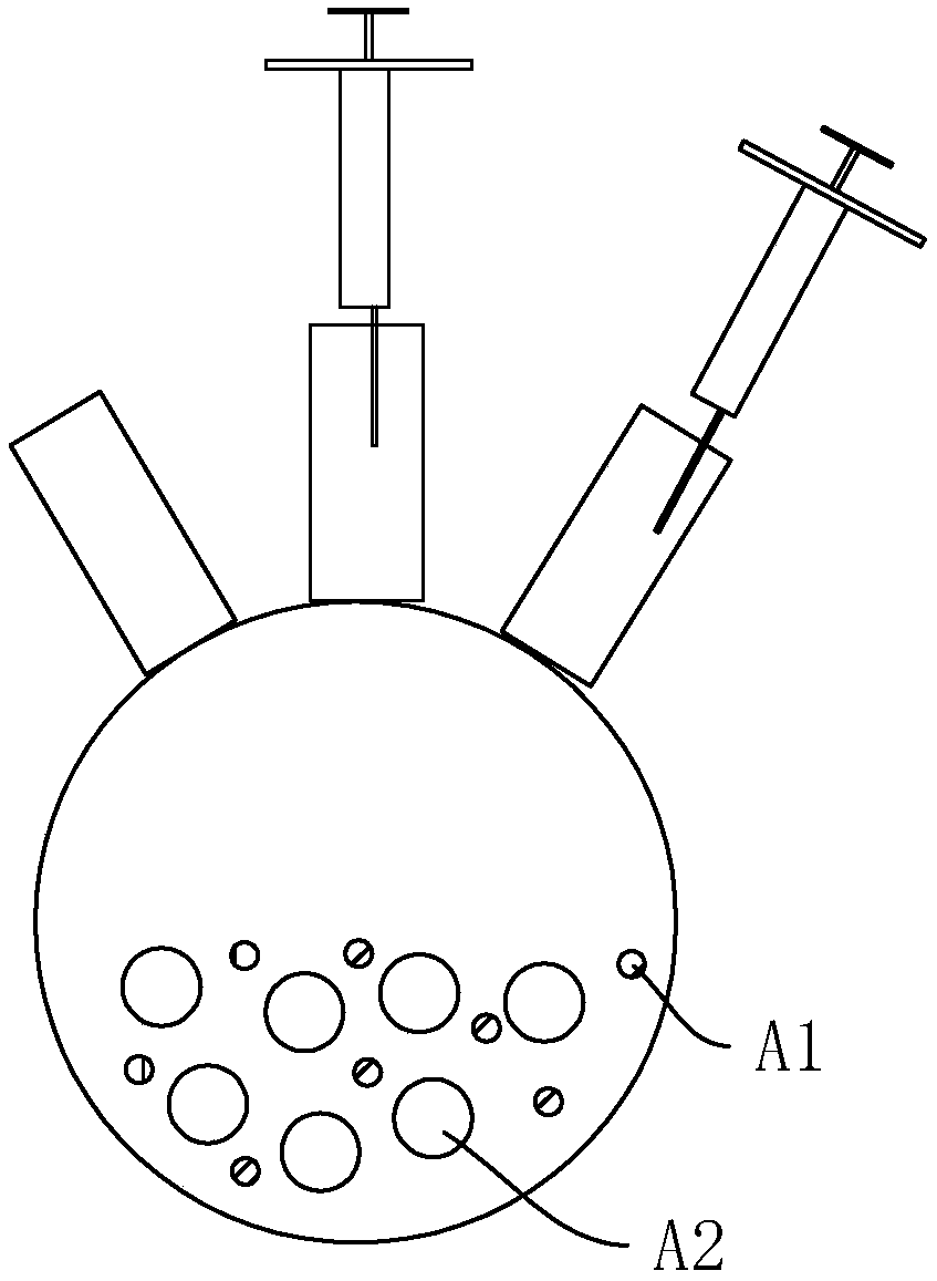
[0036] Such as figure 1 It is a schematic diagram of the one-pot synthesis method of quantum dots and nanoparticles, where A1 is nanoparticles and A2 is quantum dots.

[0037] The quantum dot light-emit...

Embodiment 2

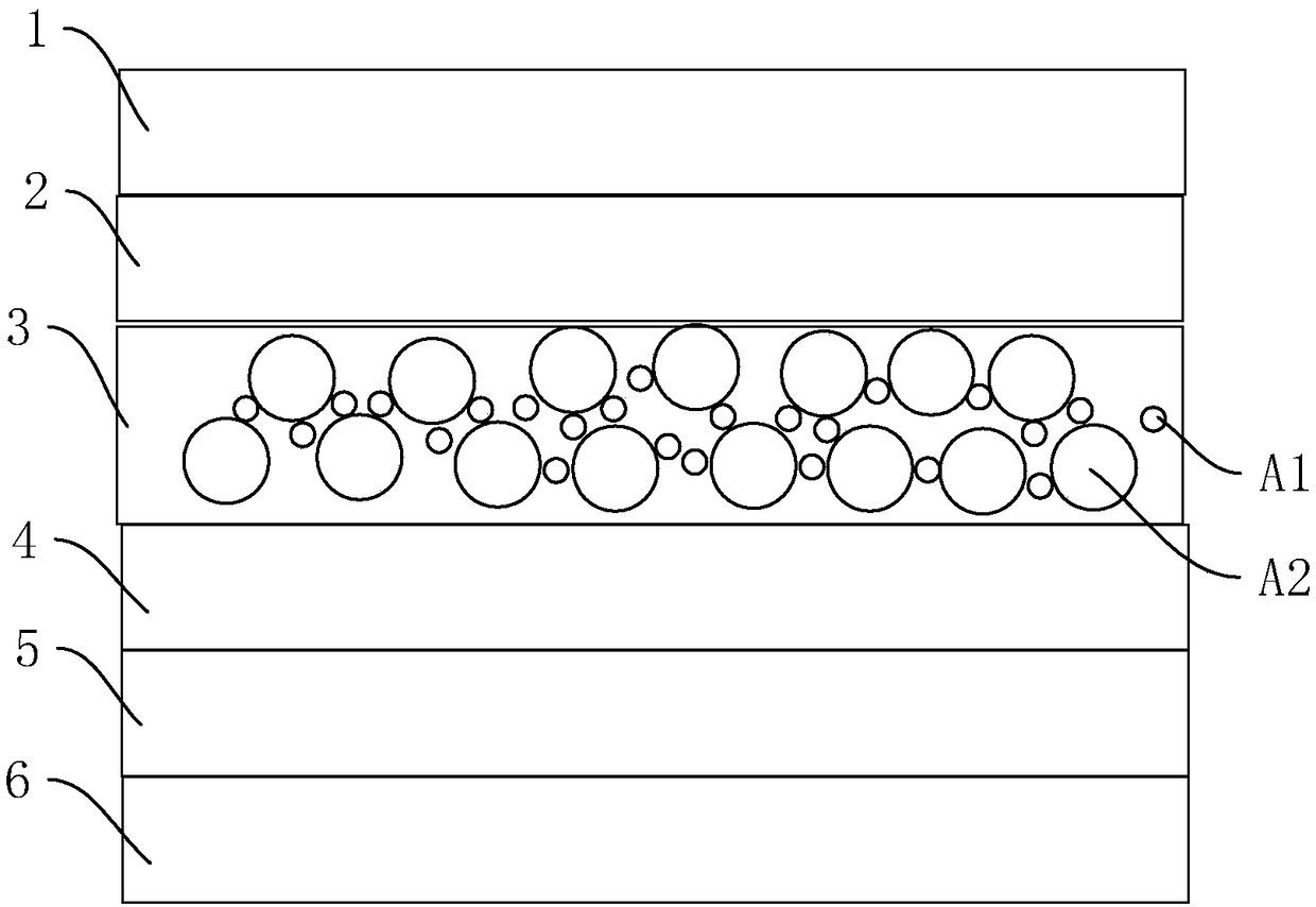
[0055] Embodiment 2, a light-emitting device using a method for preparing quantum dot light-emitting layer raw materials, referring to the figure, includes a quantum dot light-emitting diode, and a quantum dot light-emitting diode includes a first electrode layer 1 and a first charge transport layer 2 stacked in sequence from top to bottom , a quantum dot light-emitting layer 3 , a second charge transport layer 4 , a second electrode layer 5 and a substrate 6 .

[0056] When the quantum dot light-emitting diode is an upright type, the first charge transport layer 2 is a hole transport layer, and the second charge transport layer 4 is an electron transport layer; when the quantum dot light-emitting diode is an inverted type, the first charge transport layer 2 is an electron transport layer. Transport layer, the second charge transport layer 4 is a hole transport layer.

[0057] The positive and inverted quantum dot light-emitting diodes are not limited to the above-mentioned fu...


PUM

PropertyMeasurementUnit
thicknessaaaaaaaaaa
sizeaaaaaaaaaa
thicknessaaaaaaaaaa

Abstract

The invention discloses a quantum dot light-emitting layer raw material preparation method and a light-emitting device applying the method, and aims to solve the problem that the photoelectric effectof a device is influenced due to unbalanced carrier injection in an existing QLED device and the like; the key points of the technical scheme are as follows: the method comprises the following steps of 1, selecting a core of a quantum dot, wherein the core comprises one or more of an II-V group compound semiconductor, an III-V group compound semiconductor, and an IV-VI group compound semiconductor; 2, determining a shell of the quantum dots needing to be generated, wherein the shell comprises one or more of ZnS, ZnSe, CdS, CdSe, CdZnS, CdZnSe or CdZnSeS; and 3, preparing the quantum dot and carrying out a nano-particle one-pot synthesis method, wherein the quantum dot light-emitting layer raw material is prepared according to the quantum dot and the nano-particle one-pot synthesis method,based on the core selected in the step 1 and the shell selected in the step 2, so that the problem that the carrier injection of the QLED device is unbalanced and the leakage current is high can be solved, and the photoelectric effect is enhanced.

Description

technical field [0001] The invention relates to the field of photoelectric elements, more specifically, it relates to a method for preparing quantum dot light-emitting layer raw materials and a light-emitting device using the method. Background technique [0002] Quantum dot light-emitting diode (QLED) based on fluorescent semiconductor quantum dots has the advantages of simple preparation process, long life, high color purity, moderate color temperature, and good stability, and has great potential in the fields of next-generation lighting and flat panel displays application prospects. [0003] At present, under the unremitting research of the vast number of scientific researchers, both the performance parameters of quantum dot materials and quantum dot light-emitting diodes have been greatly improved. However, there are still many problems to be solved in QLED at present, especially the imbalance of electron and hole injection, which has a great impact on the lifetime and ...

Claims


Application Information

Patent Timeline
Patent Type & Authority Applications(China)
IPC IPC(8): H01L51/56H01L51/54H01L51/50B82Y30/00B82Y40/00
CPCB82Y30/00B82Y40/00H10K50/115H10K2102/00H10K71/00
Inventor 张孟李霞张超
Owner 嘉兴纳鼎光电科技有限公司
Why Eureka
Try Eureka