
Method for obtaining In quantum dot on surface of InGaN, InGaN quantum dot and epitaxial structure

A technology of epitaxial structure and quantum dots, which is applied in the direction of electrical components, circuits, semiconductor devices, etc., can solve the problems of distribution and size influence, complex process, size and density and other parameters discrete, and achieve high density, simple growth process, good The effect of size uniformity

Active Publication Date: 2019-03-12
INST OF SEMICONDUCTORS - CHINESE ACAD OF SCI
View PDF4 Cites 0 Cited by
  • Summary
  • Abstract
  • Description
  • Claims
  • Application Information

AI Technical Summary

Problems solved by technology

Among them, although the selected area growth technology can obtain quantum dots with uniform size and high density, the complex processing technology will bring inevitable additional damage to the quantum dots, and its complicated process also makes it difficult to realize practical applications.
Although the self-assembly growth method has the advantages of simple growth process, less defects and high quality of the prepared quantum dots, the large dispersion of parameters such as the position distribution, size and density of the quantum dots leads to large spectral fluctuations when it is used as an active region. widening
In recent years, it has also been proposed to use nitride nano-metal droplets to obtain InGaN quantum dots, but the difficulty of this method is how to obtain uniformly distributed nano-metal droplets, and its distribution and size will be affected by growth conditions and equipment.
[0004] In summary, the current quantum dot preparation methods are difficult to obtain high-density, high-uniformity and high-quality InGaN quantum dot materials, which seriously restricts the development and application of InGaN quantum dot devices

Method used


Image

  • Method for obtaining In quantum dot on surface of InGaN, InGaN quantum dot and epitaxial structure
  • Method for obtaining In quantum dot on surface of InGaN, InGaN quantum dot and epitaxial structure
  • Method for obtaining In quantum dot on surface of InGaN, InGaN quantum dot and epitaxial structure

Examples


Embodiment Construction

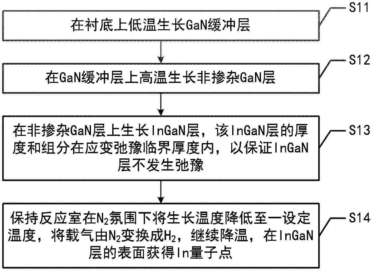
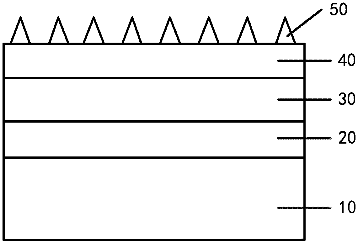
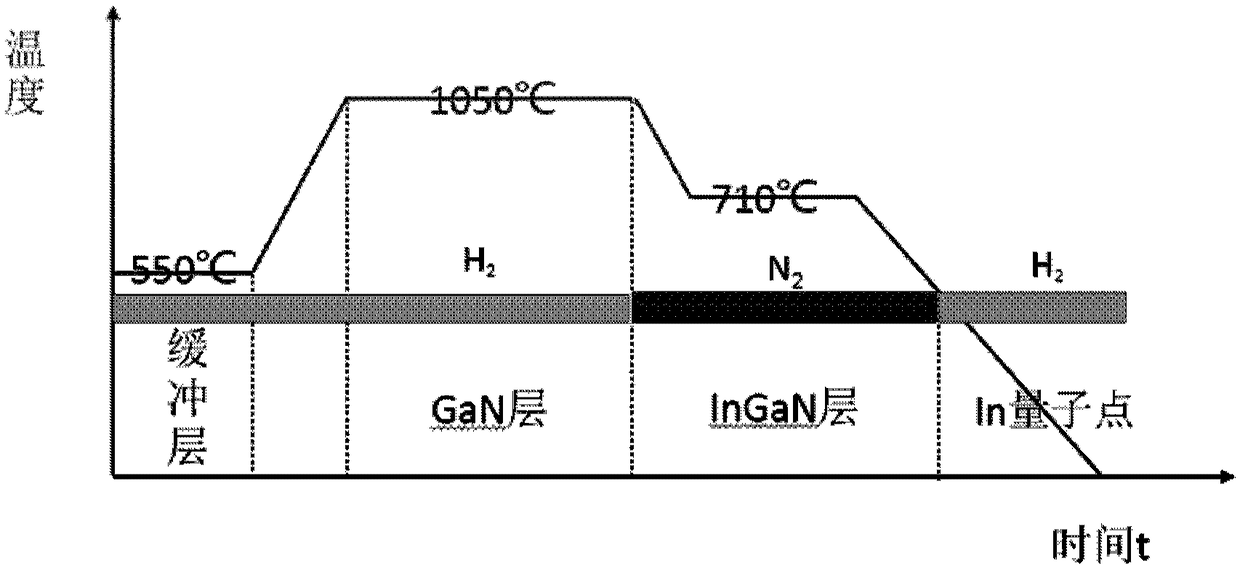
[0029] The present disclosure provides a method for obtaining In quantum dots on the surface of InGaN, InGaN quantum dots and an epitaxial structure. 2 It has high density and very good size uniformity, and the growth process is simple. It provides a uniform and reliable template for obtaining InGaN quantum dots from metal nitride droplets, and promotes the practical application of InGaN quantum dots in optoelectronic devices. . In order to make the purpose, technical solutions and advantages of the present disclosure clearer, the present disclosure will be further described in detail below in conjunction with specific embodiments and with reference to the accompanying drawings. In this disclosure, "between" includes endpoint values; "InGaN layer" and "InGaN layer" x Ga l-x N layer" is the same concept, In x Ga 1-x The N layer clearly shows the value of the In composition x.

[0030] In a first exemplary embodiment of the present disclosure, a method for obtaining In quan...


PUM


Abstract

The invention discloses a method for obtaining an In quantum dot on the surface of InGaN, an InGaN quantum dot and an epitaxial structure, wherein the method comprises the steps of: growing a GaN buffer layer on a substrate; growing an undoped GaN layer on the GaN buffer layer; growing an InGaN layer on the undoped GaN layer; and, reducing the growth temperature of a reaction chamber to the set temperature in the N2 atmosphere, converting N2 into H2, and continuously cooling, so that the In quantum dot on the surface of the InGaN layer is obtained. The In quantum dot obtained in the inventionhas high density and very good dimensional uniformity; furthermore, the growth process is simple; a uniform and reliable template is provided for obtaining the InGaN quantum dot by nitridation of metal droplets; and thus, practical application of the InGaN quantum dot in a photoelectric device is promoted.

Description

technical field [0001] The disclosure belongs to the technical field of semiconductors, and relates to a method for obtaining In quantum dots on an InGaN surface, the InGaN quantum dots and an epitaxial structure. Background technique [0002] In recent years, the preparation technology of GaN-based semiconductor materials has made great progress, which has vigorously promoted the rapid development of optoelectronic devices such as light-emitting diodes (LEDs) and laser diodes (LDs) in the visible light band. Traditional GaN-based light-emitting devices use InGaN / GaN multi-quantum well structures grown on polar planes as active regions. Although the quality of the GaN material grown on the polar plane is the highest at present, due to the quantum confinement Stark effect (QCSE) on the polar plane, this effect greatly reduces the luminous efficiency of electron-hole radiation in the quantum well structure, which seriously restricts improved the performance of light-emitting ...

Claims


Application Information

Patent Timeline
Patent Type & Authority Applications(China)
IPC IPC(8): H01L33/06H01L33/12H01L33/00
CPCH01L33/0075H01L33/06H01L33/12
Inventor 刘双韬赵德刚杨静江德生刘宗顺朱建军
Owner INST OF SEMICONDUCTORS - CHINESE ACAD OF SCI
Learn More