
Thin film material for overvoltage protection of input and output pins of integrated circuits and using method

A thin-film material and overvoltage protection technology, applied in circuits, electrical components, electrical solid devices, etc., can solve the problems of expensive products, increase chip area, increase product size, etc., and achieve the effect of adjustable threshold voltage and cost reduction

Active Publication Date: 2019-03-15
SHANGHAI YINT ELECTRONICS
View PDF12 Cites 1 Cited by
  • Summary
  • Abstract
  • Description
  • Claims
  • Application Information

AI Technical Summary

Problems solved by technology

Generally, semiconductor overvoltage protection devices such as pnpn overvoltage protection elements or pn diode elements are installed on the substrate, which greatly increases the size of the product, increases the area of ​​the chip, and makes the product expensive

Method used


Image

  • Thin film material for overvoltage protection of input and output pins of integrated circuits and using method
  • Thin film material for overvoltage protection of input and output pins of integrated circuits and using method
  • Thin film material for overvoltage protection of input and output pins of integrated circuits and using method

Examples


Embodiment Construction

[0022] Embodiments of the present invention are described below through specific examples, and those skilled in the art can easily understand other advantages and effects of the present invention from the content disclosed in this specification. The present invention can also be implemented or applied through other different specific implementation modes, and various modifications or changes can be made to the details in this specification based on different viewpoints and applications without departing from the spirit of the present invention.

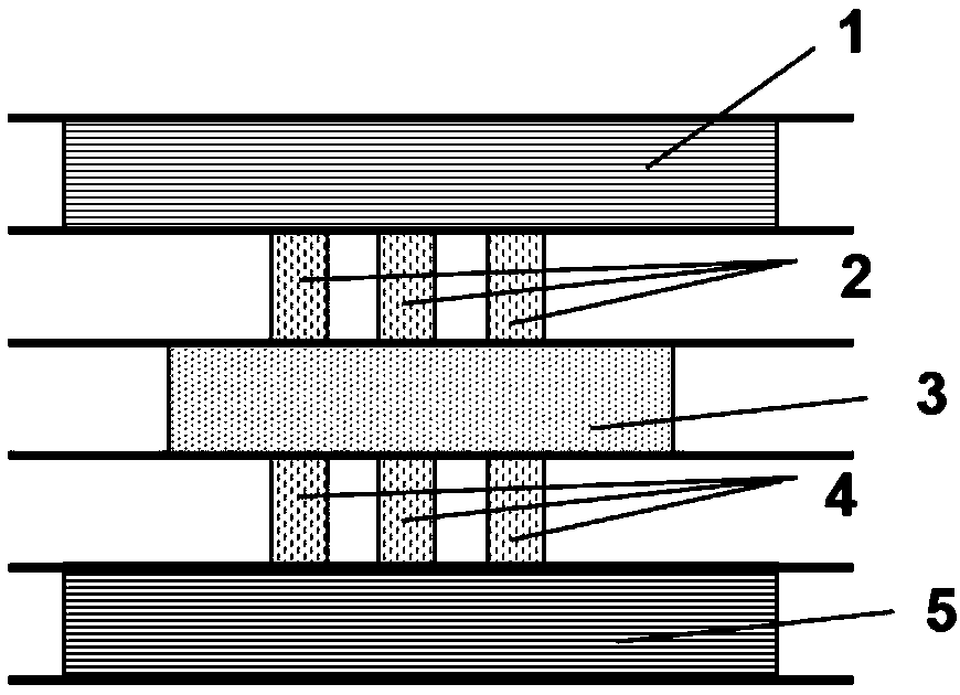
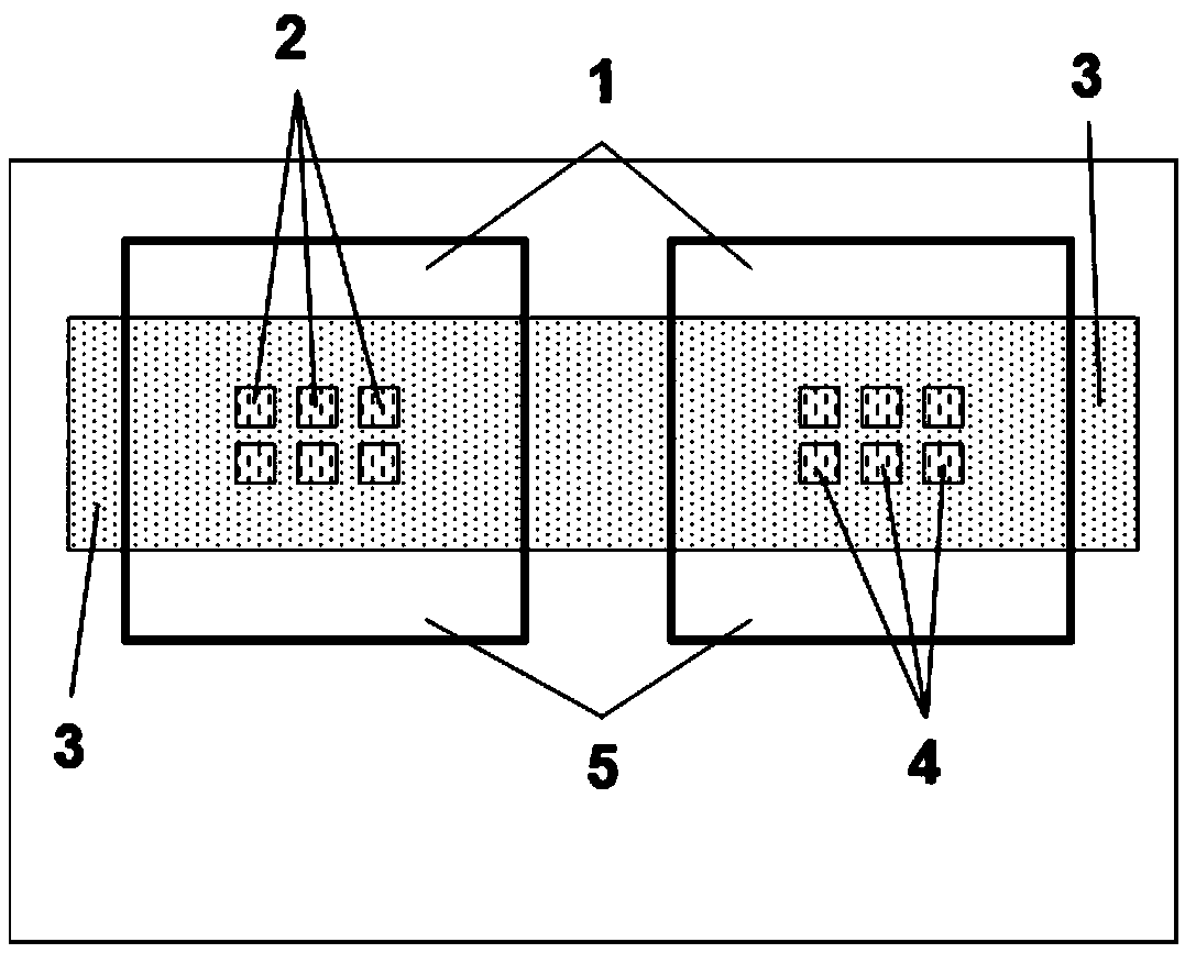
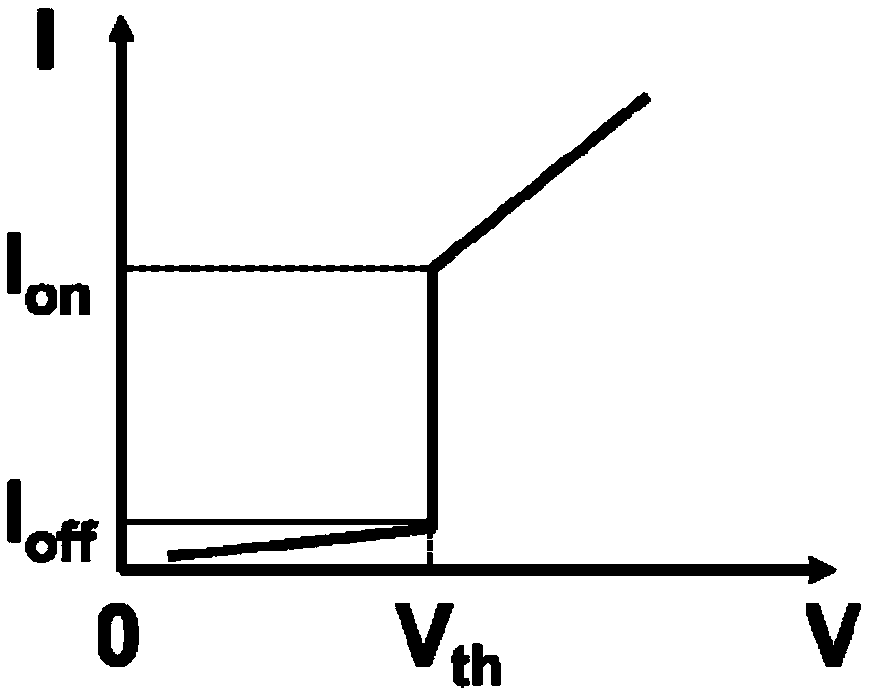
[0023] see Figure 1 to Figure 3 . It should be noted that the diagrams provided in this embodiment are only schematically illustrating the basic idea of ​​the present invention, and only the components related to the present invention are shown in the diagrams rather than the number, shape and shape of the components in actual implementation. Dimensional drawing, the type, quantity and proportion of each component can be changed arb...


PUM

PropertyMeasurementUnit
Thicknessaaaaaaaaaa

Abstract

The invention provides a thin film material for overvoltage protection of input and output pins of integrated circuits and a using method. The thin film material is a compound formed by five elements:60-90% of silicon, 35-5% of selenium, and the balance of nitrogen, germanium and arsenic; and the thin film material can be prefabricated into an alloy target through ion vapor deposition, and has athickness between 10 nm and 10 um. The using method is a low-cost strong inhibitor device design scheme for making the thin film material at pin areas of integrated circuits in a form of an overvoltage protection tape or an overvoltage protection ring, so as to prevent lightning and static impact for all the pins. By utilizing a specific threshold value breakover characteristic of the compound material, overvoltage protection is realized, so that the thin film material is novel in concept and simple in structure, and is an overvoltage protection material and device with extremely high overvoltage protection response speed and extremely strong overvoltage inhibition ability.

Description

technical field [0001] The invention relates to the field of overvoltage protection in circuits, in particular to a compound film overvoltage protection material and device used in integrated circuits. Background technique [0002] In today's information age, computer networks and communication equipment are becoming more and more sophisticated, and the requirements for their working environment are also getting higher and higher, and lightning and instantaneous overvoltage of large electrical equipment will be sent and received more and more frequently through power supplies, antennas, and radio signals. Equipment and other lines intrude into indoor electrical equipment and network equipment, causing damage to equipment or components, casualties, interference or loss of transmitted or stored data, and even misoperation or temporary paralysis of electronic equipment, system pause, data transmission interruption, LAN Even the wide area network is damaged. Overvoltage protect...

Claims


Application Information

Patent Timeline
IPC IPC(8): H01L23/482
CPCH01L23/4827
Inventor 陈小刚肖南海
Owner SHANGHAI YINT ELECTRONICS
Learn More