Supercharge Your Innovation With Domain-Expert AI Agents!

Automatic surface defect detecting device and automatic surface defect detecting method for large-opening curved-surface optical elements

An automatic detection device and technology for optical components, applied in the direction of optical components, optical testing flaws/defects, measuring devices, etc., can solve problems such as poor subjective judgment accuracy, scratches, and affecting optical system performance, and achieve detection accuracy and detection Effects of improved efficiency, improved imaging contrast and signal-to-noise ratio

Active Publication Date: 2019-03-19
INST OF OPTICS & ELECTRONICS - CHINESE ACAD OF SCI
View PDF15 Cites 12 Cited by
  • Summary
  • Abstract
  • Description
  • Claims
  • Application Information

AI Technical Summary

Problems solved by technology

After grinding and polishing, the surface of curved optical components often has various defects (such as scratches, depressions, cracks, chipping and other surface defects), these defects will not only reduce the user experience, but even affect the performance of the optical system
[0003] The surface defect detection of large-caliber curved optical components is still dominated by manual qualitative detection. The current mainstream manual visual inspection is not only inefficient, but also has poor subjective judgment accuracy, which seriously restricts the automation process of advanced optical manufacturing.
In recent years, the defect detection technology based on machine vision has attracted the attention of many researchers, but the current method has low detection accuracy and takes a long time, which cannot meet the real-time detection needs of the current industrial site.
And it is powerless to detect surface defects on curved surfaces

Method used


Image

  • Automatic surface defect detecting device and automatic surface defect detecting method for large-opening curved-surface optical elements
  • Automatic surface defect detecting device and automatic surface defect detecting method for large-opening curved-surface optical elements
  • Automatic surface defect detecting device and automatic surface defect detecting method for large-opening curved-surface optical elements

Examples


Embodiment Construction

[0025] The present invention will be described in detail below in conjunction with the accompanying drawings and specific embodiments.

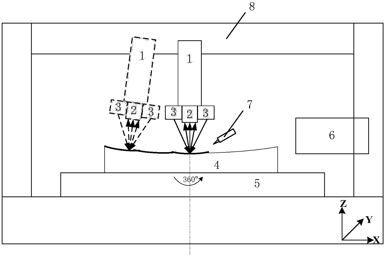
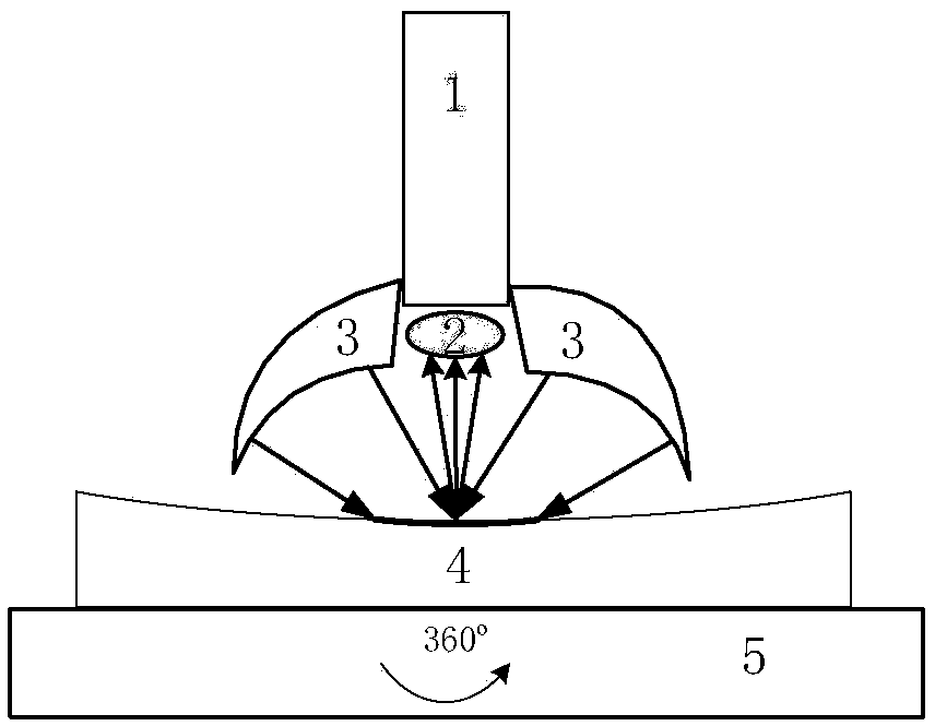
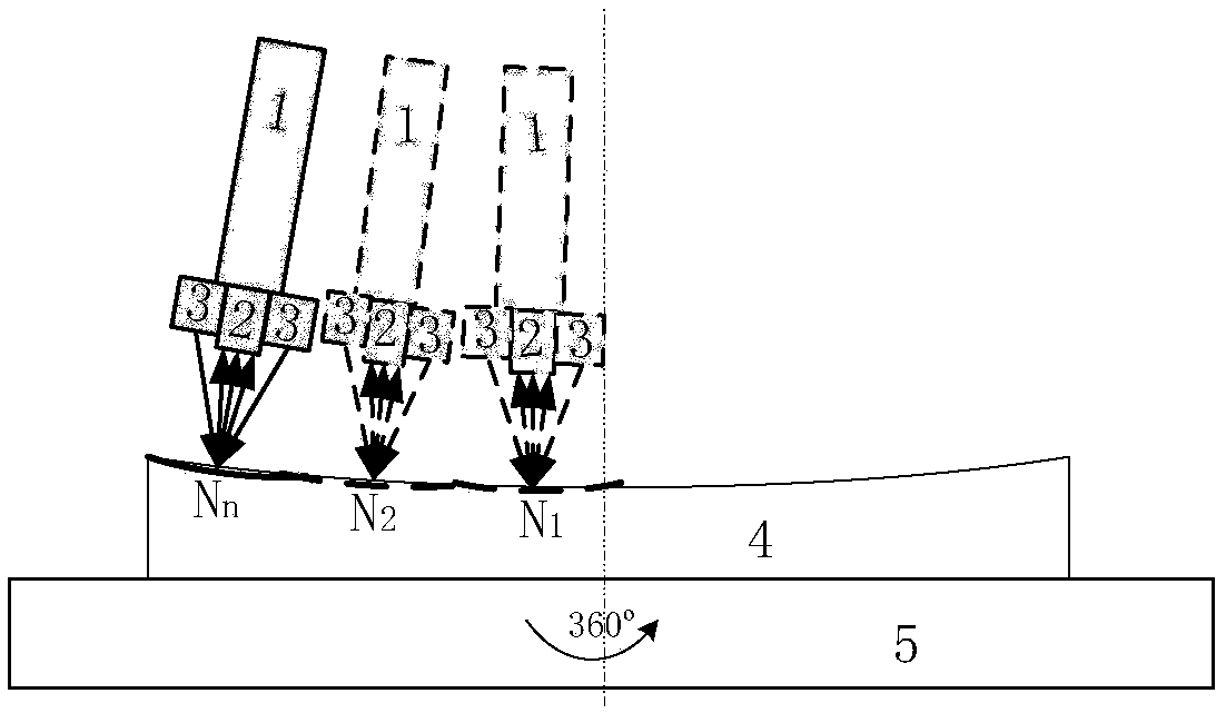
[0026] Such as figure 1 As shown, in the embodiment of the present invention, an automatic detection device for surface defects of a large-diameter curved optical element includes a sensor system 1, an imaging system 2, an illumination system 3, a large-diameter optical element 4, a rotating workpiece table 5, and an automatic sampling device 6. Spray device 7, guide rail 8. Among them, the large-diameter optical element 4 is placed on the workpiece table 5 that can rotate 360 ​​degrees around the Z axis. The sensor system 1, the imaging system 2, and the lighting system 3 form a measuring head. The measuring head is vertically installed on the guide rail 8 to realize the large-diameter optical The multi-axis linkage of the component, including the translation along the X and Z axes and the swing around the Y axis, ensures that the optical a...


PUM


Abstract

The invention relates to an automatic surface defect detecting device and an automatic surface defect detecting method for large-opening curved-surface optical elements, and belongs to the technical field of photoelectric detection. The automatic surface defect detecting device comprises a measuring head, a rotary worktable, an automatic sampling device and a spraying device. The measuring head comprises a sensor system, an illuminating system and an imaging system, the illuminating system is used for providing high-uniformity and high-luminance illumination for a surface of a detected sample,and the rotary worktable and the imaging system are used for performing annular scanning and high-resolution scattering imaging on defects in an optical surface area. The automatic sampling device isused for automatically clamping an optical element by a mechanical arm in automated production. Once only foreign matters such as dust and impurities are detected on a surface of the optical element,the spraying device is activated to remove the pseudo-flaws including the dust and the impurities accurately. The automatic surface defect detecting device and the automatic surface defect detectingmethod for the large-opening curved-surface optical elements solve the problem that detection of defects on the surfaces of the large-opening curved-surface optical elements is difficult and low in efficiency, and the surface defects on large-opening plane-surface optical elements, large-opening spherical-surface optical elements and large-opening aspheric-surface optical elements can be measuredquickly.

Description

technical field [0001] The invention belongs to the field of advanced optical manufacturing and detection, and relates to an optical detection device, in particular to an automatic detection device and method for surface defects of large-caliber curved optical elements. Background technique [0002] With the continuous development of advanced optical manufacturing technology, application fields such as microelectronics equipment, aerospace, precision measurement and laser systems have put forward higher technical requirements for the surface processing quality of precision optical components, which are their core components. After grinding and polishing, the surface of curved optical components often has various defects (such as scratches, depressions, cracks, chipping and other surface defects), these defects will not only reduce the user experience, but even affect the performance of the optical system. [0003] The surface defect detection of large-aperture curved optical...

Claims


Application Information

Patent Timeline
IPC IPC(8): G01N21/88
CPCG01N21/8851G01N2021/8887H01L22/12G01N2021/9511G01N21/95G02B7/1827G01N21/8806G01N21/94G01N21/9501G01N21/95607G06K7/10732G06T7/001G06T2207/30148
Inventor 全海洋徐富超付韬韬胡小川吴高峰侯溪伍凡李声
Owner INST OF OPTICS & ELECTRONICS - CHINESE ACAD OF SCI
Features
  • R&D
  • Intellectual Property
  • Life Sciences
  • Materials
  • Tech Scout
  • Unparalleled Data Quality
  • Higher Quality Content
  • 60% Fewer Hallucinations
Learn More