A SoC prototype verification method based on FPGA

A prototype verification, interface control module technology, applied in the direction of instruments, electrical digital data processing, computing, etc., can solve problems such as low visibility of test signals, and achieve the effect of shortening implementation time, high practical value, and reducing FPGA storage resources

Active Publication Date: 2019-03-19
BEIJING INST OF REMOTE SENSING EQUIP
View PDF6 Cites 4 Cited by
  • Summary
  • Abstract
  • Description
  • Claims
  • Application Information

AI Technical Summary

Problems solved by technology

[0003] The object of the present invention is to provide a kind of SoC prototype verification method based on FPGA,

Method used


Image

  • A SoC prototype verification method based on FPGA

Examples


Embodiment Construction

[0025] A kind of concrete steps of SoC prototype verification method based on FPGA are:

[0026] The first step is to build a SoC prototype verification system

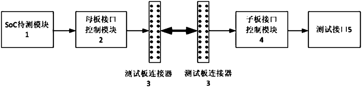
[0027] The SoC prototype verification system includes: a SoC module to be tested 1 , a motherboard interface control module 2 , a test board connector 3 , a daughter board interface control module 4 and a test interface 5 .

[0028] The Soc module 1 to be tested is connected to the motherboard interface control module 2, the motherboard interface control module 2 is connected to the test board connector 3, the test board connector 3 is connected to the daughter board interface control module 4, and the daughter board interface control module 4 is connected to the test board Interface 5 is connected. There are multiple test interfaces 5 .

[0029] The function of the Soc module 1 to be tested is to simulate the function of the SoC chip, and connect the signal to be tested with the motherboard interface control module...


PUM


Abstract

The invention discloses a SoC prototype verification method based on FPGA. The prototype verification system adopted is composed of a motherboard and a daughter board. The FPGA of the motherboard comprises a SoC module to be tested (1) and a motherboard interface control module (2). The daughter board is connected with the motherboard through a test connector (3); the daughter board FPGA comprisesa daughter board interface control module (4) and a test interface (5). A motherboard interface control module (2) compresses and sends signals of modules to be tested to a daughter board interface control module (4) by using a time division multiplexing technology, and the daughter board interface control module (4) extracts and analyzes signals to be distributed to a test interface (5), and thetest interface (5) is connected with a test device. This method is free from the prototype verification system FPGA storage resources are limited, using the built-in logic analyzer tool ChipScope subject to test signal bit width, sampling depth limit. As ChipScope is not needed, it can significantly reduce the utilization rate of FPGA memory resources, shorten the FPGA implementation process, andhas high practical value for improving the verification and test efficiency.

Description

technical field [0001] The invention relates to a SoC prototype verification method, in particular to an FPGA-based SoC prototype verification method. Background technique [0002] FPGA-based prototype verification has become one of the mainstream SoC verification methods because it can significantly improve SoC verification efficiency and shorten the SoC development cycle. However, as the scale of SoC continues to increase, in previous methods, prototype verification is limited by FPGA storage resources, which leads to restrictions on the test signal bit width and sampling depth when using ChipScope, thus making the test signal visibility of FPGA-based prototype verification Decreased significantly. In order to observe more signals, ChipScope has to be modified repeatedly, and synthesis, layout and routing are repeated, which reduces the efficiency of prototype verification and greatly reduces the value of SoC prototype verification. SoC is a system on a chip, and ChipSco...

Claims


Application Information

Patent Timeline
IPC IPC(8): G06F11/273
CPCG06F11/273
Inventor 赵晨旭刘志哲郭广浩
Owner BEIJING INST OF REMOTE SENSING EQUIP
Why Eureka
Try Eureka