
6t storage unit structure of sram

A technology of memory cells and active areas, applied in electrical components, semiconductor devices, transistors, etc., can solve the problems of device mismatch, affecting device matching, and inconsistency in dimensional changes, so as to eliminate the mismatch in width and length, improve Good matching and consistency

Active Publication Date: 2021-04-13
SHANGHAI HUALI INTEGRATED CIRCUIT CORP
View PDF3 Cites 0 Cited by
  • Summary
  • Abstract
  • Description
  • Claims
  • Application Information

AI Technical Summary

Problems solved by technology

Depend on image 3 It can be seen that, although the width change of the active region 201a is at a right angle during the layout design, after the actual active region definition process, the width change of the active region 201a will follow the dotted line shown by the mark 108 change, the length of the active region covered by the change range of the dotted line 108 is relatively large, and will extend from the bottom of the polysilicon gate 202 of the second NMOS transistor 106, that is, the channel region, along the length direction of the channel region to the In the channel region of the second selection transistor 102, this will cause the length and width of the channel regions of the second NMOS transistor 106 and the second selection transistor 102 to change, and this variation is due to the actual process. , so as the process conditions change, the change of the channel region of the corresponding transistor will also be inconsistent, that is, the size change of the channel region of the transistor at different positions of the chip produced in the same batch will be inconsistent, and the change of the channel region of the transistor produced in different batches will be inconsistent. The size variation of the channel region of each transistor between chips will be more inconsistent, which will affect the matching of the device, that is, it is easy to generate device mismatch, which will affect the minimum read voltage (Vmin) of the device and the yield of the product

Method used


Image

  • 6t storage unit structure of sram
  • 6t storage unit structure of sram
  • 6t storage unit structure of sram

Examples


Embodiment Construction

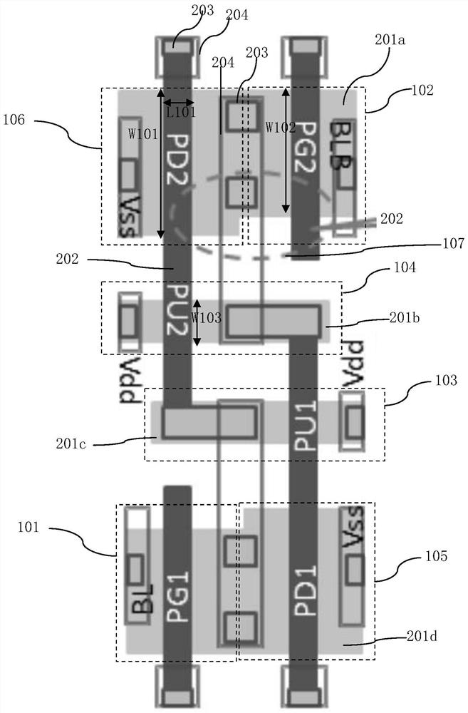
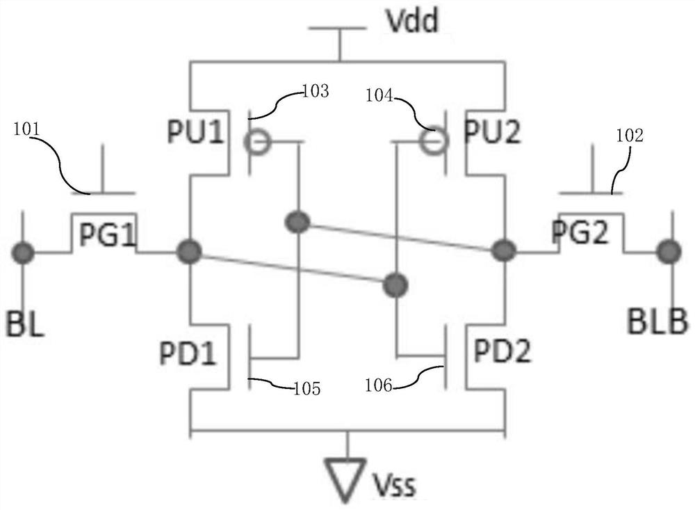
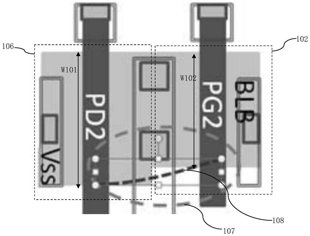
[0061] Such as Figure 4 Shown is the layout of the 6T memory cell structure of the SRAM of the embodiment of the present invention; Figure 5 yes Figure 4 The circuit diagram of the 6T memory cell structure of the SRAM in the embodiment of the present invention is shown, the 6T memory cell structure of the SRAM in the embodiment of the present invention consists of a first selection transistor 1, a second selection transistor 2, a first PMOS transistor 3, and a second PMOS transistor 4 The first NMOS transistor 5 and the second NMOS transistor 6 are connected to form six transistors, the first PMOS transistor 3 and the second PMOS transistor 4 are used as two pull-up transistors (Pull Up, PU), and the The first NMOS transistor 5 and the second NMOS transistor 6 serve as two pull down transistors (Pull Down, PD). Figure 4 Among them, the first selection transistor 1 is also represented by PG1, the second selection transistor 2 is also represented by PG2, the first PMOS tra...


PUM


Abstract

The invention discloses a 6T storage unit structure of SRAM, which is composed of first and second selection transistors, first and second PMOS transistors, first and second NMOS transistors connected to form a 6T storage unit structure, and the two selection transistors are respectively formed in In the first and second active regions; two PMOS transistors are formed in the third active region; two NMOS transistors are formed in the fourth active region; both the first and second active regions have a first width, and The three active regions have a second width, the fourth active region has a third width, and the third width is greater than the first width and greater than the second width, so as to optimize the circuit read window and write window, and the transistors with the same channel region width are arranged in In the same active area, each active area adopts the setting of the same width, which can prevent the width of the active area from gradually changing. The invention can eliminate the influence of the width change of the active region on the channel length and width of the transistor, thereby improving the matching degree between devices and thereby improving the yield rate and increasing the process window.

Description

technical field [0001] The invention relates to a semiconductor integrated circuit, in particular to a 6T storage unit structure of an SRAM. Background technique [0002] Such as figure 1 Shown is the layout of the 6T memory cell structure of the existing SRAM; figure 2 yes figure 1 The circuit diagram of the 6T memory cell structure of the existing SRAM shown, the 6T memory cell structure of the existing SRAM is composed of the first selection transistor 101, the second selection transistor 102, the first PMOS transistor 103, the second PMOS transistor 104, the first NMOS transistor The first PMOS transistor 103 and the second PMOS transistor 104 are used as two pull-up transistors (Pull Up, PU). The first NMOS transistor 105 and the second NMOS transistor 106 serve as two pull down transistors (Pull Down, PD). figure 1 Among them, the first selection transistor 101 is also represented by PG1, the second selection transistor 102 is also represented by PG2, the first PM...

Claims


Application Information

Patent Timeline
Patent Type & Authority Patents(China)
IPC IPC(8): H01L27/11H01L27/02H10B10/00
CPCH01L27/0207H10B10/12
Inventor 周晓君
Owner SHANGHAI HUALI INTEGRATED CIRCUIT CORP
Learn More