A kind of sonos storage structure and its manufacturing method

A storage structure and manufacturing method technology, applied in information storage, read-only memory, static memory, etc., can solve the problems of reducing the size of planar transistors, and achieve better leakage performance, simple manufacturing process, and better uniformity Effect

Active Publication Date: 2022-01-04
SHANGHAI HUALI MICROELECTRONICS CORP
View PDF17 Cites 0 Cited by
  • Summary
  • Abstract
  • Description
  • Claims
  • Application Information

AI Technical Summary

Problems solved by technology

As the size of VLSI continues to shrink, the limitations on manufacturing process and material properties are becoming more and more significant, making it more and more difficult to reduce the size of planar transistors

Method used


Image

  • A kind of sonos storage structure and its manufacturing method
  • A kind of sonos storage structure and its manufacturing method
  • A kind of sonos storage structure and its manufacturing method

Examples


Embodiment Construction

[0086] The present invention will be described in detail below in conjunction with the accompanying drawings and specific embodiments. Note that the aspects described below in conjunction with the drawings and specific embodiments are only exemplary, and should not be construed as limiting the protection scope of the present invention.

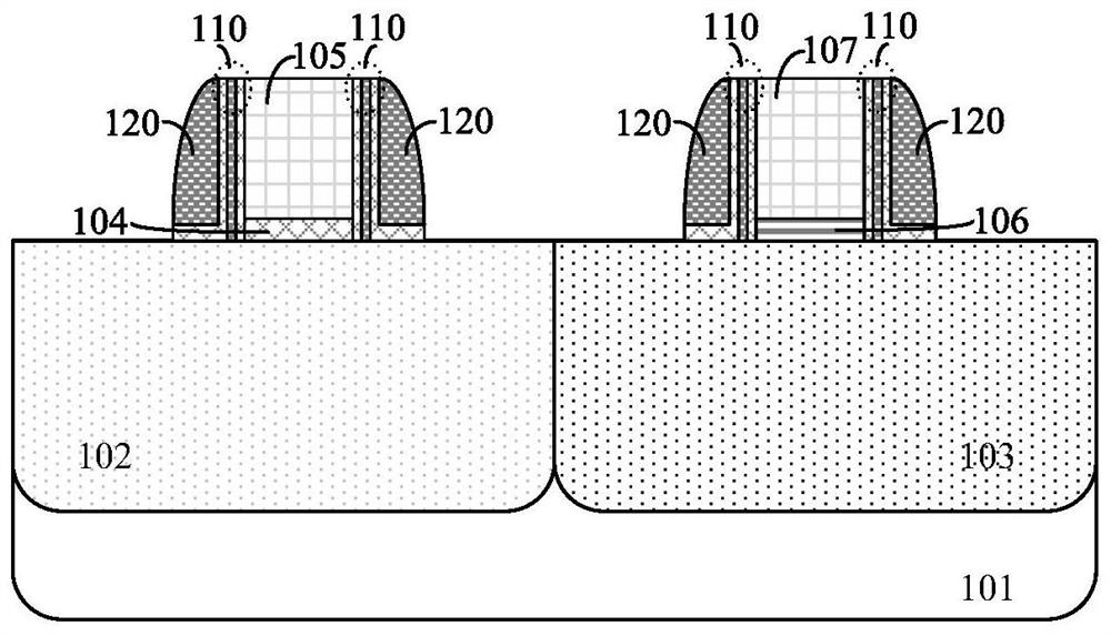
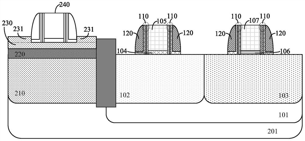
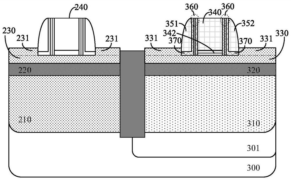
[0087] The present invention relates to semiconductor technology and devices. More specifically, an embodiment of the present invention provides a semiconductor device. The semiconductor device is a SONOS memory cell formed on the surface of SOI. Each SONOS memory cell includes a storage transistor gate, a first select transistor gate and a select transistor second gate. Grid, the first grid of the selection transistor and the second grid of the selection transistor are located on both sides of the grid of the storage tube, and the first grid of the selection transistor, the second grid of the selection transistor and the grid of the storage t...


PUM


Abstract

The invention provides a SONOS storage structure and a manufacturing method thereof. The SONOS storage structure includes a substrate and a selection transistor gate and a storage transistor gate formed on the substrate, wherein the substrate is a composite substrate including a silicon base Layer, buried oxide layer and silicon surface layer, the upper part of the silicon base layer is the storage tube well region; the selection tube grid and the storage tube grid are formed on the silicon surface layer; the selection tube grid includes the first grid of the selection tube and the first grid of the selection tube. The second grid of the selection transistor, the first grid of the selection transistor and the second grid of the selection transistor are respectively located on both sides of the grid of the storage tube, and are electrically isolated from the grid of the storage tube by the first sidewalls on both sides of the grid of the storage tube and a silicon epitaxial layer adjacent to the first gate of the selection transistor and the second gate of the selection transistor is respectively formed on the upper surface of the silicon surface layer outside the first gate of the selection transistor and the second gate of the selection transistor. The manufacturing method provided by the present invention is compatible with the existing FDSOI process, and can manufacture the above-mentioned SONOS storage unit with smaller structure and better performance.

Description

technical field [0001] The invention relates to the field of semiconductor devices and manufacturing thereof, in particular designing a SONOS storage structure and a manufacturing method thereof. Background technique [0002] Since the early days when Dr. Jack Kilby of Texas Instruments invented the integrated circuit, scientists and engineers have made numerous inventions and improvements in semiconductor devices and processes. Over the past 50 years, there has been a significant reduction in the size of semiconductors, which translates into ever-increasing processing speeds and ever-decreasing power consumption. So far, the development of semiconductors has roughly followed Moore's Law, which roughly states that the number of transistors in a dense integrated circuit doubles about every two years. Now, the semiconductor process is developing below 20nm, and some companies are working on the 14nm process. Here is just a reference, a silicon atom is about 0.2nm, which mean...

Claims


Application Information

Patent Timeline
Patent Type & Authority Patents(China)
IPC IPC(8): H01L27/11568
CPCH10B43/30H01L27/1207H01L29/40117H01L29/792H01L21/84H10B43/40H01L21/02532H01L21/26513H01L21/7624H01L27/0207H01L27/1203H01L29/42344H01L29/513H01L29/518H01L29/6653H01L29/6656H01L29/66833H01L29/7831H01L29/66484H01L21/2815G11C16/0466H01L29/511H01L29/512H10B43/35
Inventor 唐小亮陈广龙辻直树邵华
Owner SHANGHAI HUALI MICROELECTRONICS CORP
Why Eureka
Try Eureka