
Image sensor and forming method thereof

An image sensor and graphics layer technology, applied in the direction of electric solid-state devices, semiconductor devices, electrical components, etc., can solve problems affecting the performance of image sensors, etc., and achieve the effect of reducing center offset, reducing influence, and reducing dark current

Active Publication Date: 2019-04-02
淮安西德工业设计有限公司
View PDF4 Cites 9 Cited by
  • Summary
  • Abstract
  • Description
  • Claims
  • Application Information

AI Technical Summary

Problems solved by technology

[0004] However, with the improvement of device integration, the density of pixel units in the image sensor increases, and the dark current between adjacent pixel units continues to increase, which affects the performance of the image sensor.

Method used


Image

  • Image sensor and forming method thereof
  • Image sensor and forming method thereof
  • Image sensor and forming method thereof

Examples


Embodiment Construction

[0028] As mentioned in the background, prior art image sensors perform poorly.

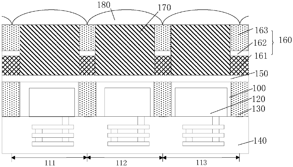
[0029] refer to figure 1 , figure 1 It is a structural schematic diagram of an image sensor, the image sensor includes a plurality of pixel units, and the pixel unit includes: an interconnection structure 140, a substrate 100, a photosensitive structure 120 and a photosensitive structure, and the substrate 100 has an opposite first surface and a second surface, the photosensitive structure 120 is located in the substrate 100, the first surface of the substrate 100 exposes the photosensitive structure 120, and the interconnect structure 140 is in contact with the first surface of the substrate 100, so The light-receiving structure is located on the second surface of the substrate 100, and the light-receiving structure includes a lens layer 180, a filter layer 170 and a grid layer 160. The lens layer 180 is located on the surface of the filter layer 170, and the grid layer 160 is located on the adj...


PUM


Abstract

The invention discloses an image sensor and a forming method thereof. The image sensor comprises a semiconductor substrate, a light sensing structure, a blocking layer and a light filtering layer, wherein the semiconductor substrate comprises a plurality of pixel areas and isolation areas located between the adjacent pixel areas; the semiconductor substrate is provided with a first surface and a second surface which are opposite to each other; the light sensing structure is located in the pixel areas of the semiconductor substrate, and the first surface of the semiconductor substrate exposes the light sensing structure; the blocking layer is located on the surface of the second surface of the semiconductor substrate, and a first groove is formed in the blocking layer, and the bottom of thefirst groove exposes the surface of the blocking layer located in the pixel areas, wherein the blocking layer is made of a pressure-resistant material; and the light filtering layer is located in thefirst groove, wherein the thermal expansion coefficient of the blocking layer material is less than that of the light filtering layer material. The performance of the image sensor is improved.

Description

technical field [0001] The invention relates to the field of semiconductor manufacturing, in particular to an image sensor and a forming method thereof. Background technique [0002] An image sensor is a semiconductor device that converts light signals into electrical signals. Image sensors are classified into complementary metal oxide (CMOS) image sensors and charge coupled device (CCD) image sensors. CMOS image sensor has the advantages of simple process, easy integration of other devices, small size, light weight, low power consumption and low cost. Therefore, with the development of image sensing technology, CMOS image sensors are increasingly used in various electronic products instead of CCD image sensors. At present, CMOS image sensors have been widely used in still digital cameras, digital video cameras, medical imaging devices, and automotive imaging devices. [0003] CMOS image sensors include front illuminated (FSI) image sensors and back illuminated (BSI) imag...

Claims


Application Information

Patent Timeline
Patent Type & Authority Applications(China)
IPC IPC(8): H01L27/146
CPCH01L27/1462H01L27/14621H01L27/14685
Inventor 龙海凤李天慧藤井光一黄晓橹夏睿
Owner 淮安西德工业设计有限公司
Features
  • Generate Ideas
  • Intellectual Property
  • Life Sciences
  • Materials
  • Tech Scout
  • Unparalleled Data Quality
  • Higher Quality Content
  • 60% Fewer Hallucinations
Learn More