Method for manufacturing semiconductor component for electric nozzle

A manufacturing method and semiconductor technology, applied to electrical components, circuits, jet propulsion devices, etc., can solve the problems of large energy loss and difficult processing, and achieve low energy loss, low processing difficulty, and prevent breakdown.

Active Publication Date: 2019-04-09
四川泛华航空仪表电器有限公司
View PDF4 Cites 0 Cited by
  • Summary
  • Abstract
  • Description
  • Claims
  • Application Information

AI Technical Summary

Problems solved by technology

[0006] In order to solve the technical problems of high processing difficulty and large energy loss in the semiconductor components used in the electric nozzle in the prior art

Method used


Image

  • Method for manufacturing semiconductor component for electric nozzle

Examples


Embodiment 1

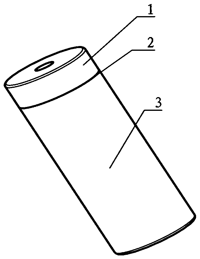
[0016] Such as figure 1 As shown, a method for manufacturing a semiconductor component for an electric nozzle described in this embodiment is characterized in that it includes the following steps: carbonizing the silicon carbide semiconductor 1, the sintered composite material 2, and the high-alumina porcelain 3 at room temperature Silicon semiconductor 1 is on top, sintered composite material 2 is in the middle, and high-alumina porcelain 3 is on the bottom. Preliminary molding is carried out to form a component to be sintered; the component to be sintered is sintered at 1800°C for two hours by hot isostatic pressing to make a semiconductor component .

[0017] In this embodiment, by integrally sintering the semiconductor and the insulator into a semiconductor component, avoiding the need to process and connect the silicon carbide semiconductor 1 and the insulator of the electric nozzle when installing in the electric nozzle, which reduces the difficulty of processing; by com...

Embodiment 2

[0019] On the basis of above-mentioned embodiment, propose embodiment 2, as figure 1 As shown, it is characterized in that: in the semiconductor component, the thickness of the silicon carbide semiconductor 1 is not greater than 5mm.

[0020] By controlling the ratio of silicon carbide semiconductor 1, sintered composite material 2, and high-alumina porcelain 3, the thickness of silicon nitride semiconductor is not greater than 5mm, and the overall height of the semiconductor component is filled by adjusting the thickness of high-alumina porcelain 3. It meets the needs of electric nozzles for semiconductor components, and has good corrosion resistance. At the same time, it can reduce the possible internal leakage current and further reduce the energy loss of electric nozzles.

[0021] In this embodiment, the use ratio of the sintered composite material 2 is relatively flexible. It is only necessary to make the sintered composite material 2 between the silicon carbide semicondu...


PUM

PropertyMeasurementUnit
thicknessaaaaaaaaaa

Abstract

The invention provides a method for manufacturing a semiconductor component for an electric nozzle, characterized in that the method includes the following steps: carrying out preliminary forming on asilicon carbide semiconductor (1), a sintered composite material (2) and alumina porcelain (3) at room temperature according to the combination order that the silicon carbide semiconductor (1) is located on the upper part, the sintered composite material (2) is located in the middle part, and the alumina porcelain (3) is located on the lower part, and further forming a to-be-sintered component; and sintering the to-be-sintered component by hot isostatic pressure at 1800DEG C for two hours to manufacture the semiconductor component. According to the scheme of the invention, a semiconductor andan insulator are integrally sintered into the semiconductor component, so that the processing difficulty is reduced; the sintered composite material (2) is added between the silicon carbide semiconductor (1) and the alumina porcelain (3), the thickness of the silicon carbide semiconductor (1) is reduced, and thus the energy loss is reduced; and the technical problem that the semiconductor component for the electric nozzle in the prior art has large processing difficulty and high energy loss can be solved.

Description

technical field [0001] The invention relates to a manufacturing method, in particular to a manufacturing method of a semiconductor component used for an electric nozzle. Background technique [0002] The electric nozzle is an important part of the ignition system of the aero-engine. Its function is to convert the high-voltage electric energy pulse generated by the ignition device into an electric spark at its end to ignite the combustible gas mixture in the engine combustion chamber. At present, the electric nozzles used in aero-engines are roughly divided into the following four types: high-pressure air gap electric nozzles, electro-erosion electric nozzles, creeping electric nozzles and semiconductor electric nozzles. [0003] The semiconductor component is an important part of the semiconductor nozzle. Its function is that under the applied voltage, the surface of the semiconductor component forms an electrical conduction, and a certain current is formed, resulting in an ...

Claims


Application Information

Patent Timeline
Patent Type & Authority Applications(China)
IPC IPC(8): H01T13/02F02C7/266
CPCF02C7/266H01T13/02
Inventor 李慧尚振杰刘涛刘宝林
Owner 四川泛华航空仪表电器有限公司
Why Eureka
Try Eureka