An optical component and its manufacturing method

An optical component and manufacturing method technology, applied in the field of optical communication, can solve problems such as failure, unfavorable clamp clamping, small lens size, etc., and achieve the effect of precise coupling or collimation and avoiding lens position deviation

Active Publication Date: 2020-12-15
INNOLIGHT TECHNOLOGY (SUZHOU) LTD
View PDF12 Cites 0 Cited by
  • Summary
  • Abstract
  • Description
  • Claims
  • Application Information

AI Technical Summary

Problems solved by technology

This can lead to overall device performance degradation or failure
[0003] In addition, in a small package, the size of the lens itself is small, and the side cutting (such as silicon lens or batch molded lens) may cause the side of the lens to have a tilt angle during mass production, which is not conducive to clamping during assembly

Method used


Image

  • An optical component and its manufacturing method
  • An optical component and its manufacturing method
  • An optical component and its manufacturing method

Examples


Embodiment 1

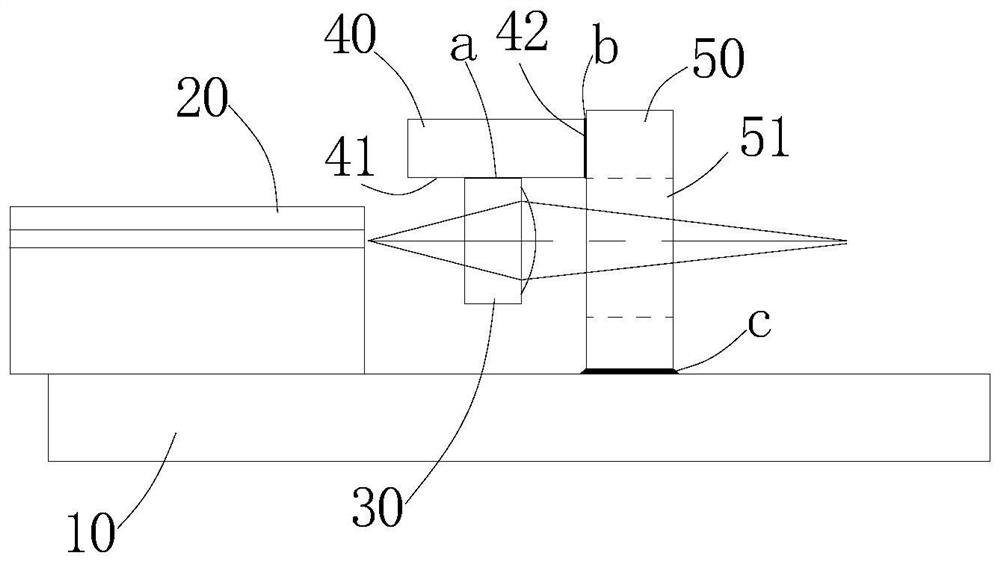
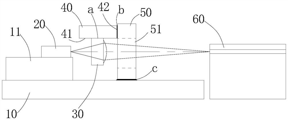
[0059] Specifically, such as figure 2 In the illustrated embodiment 1, the optical component in this embodiment includes a light emitting end. The light emitting end includes a semiconductor laser as a light-extracting element 20 , a lens element 30 and an optical waveguide 60 . Wherein, the semiconductor laser is fixed on the substrate 10 through a small substrate 11, and the lens element 30 is installed on the substrate 10 through the above-mentioned auxiliary member 40 and the support member 50. Here, the lens element 30 is a coupling lens, which can be a large power ball lens or an aspheric lens. lens etc. The optical signal emitted by the semiconductor laser is coupled into the optical waveguide 60 through the lens element 30 . The above-mentioned optical waveguide 60 may also be an optical integrated chip, optical fiber or other media for transmitting optical signals. Here, the substrate 10 may be a plane of the package housing, or may be a heat sink or other flat pl...

Embodiment 2

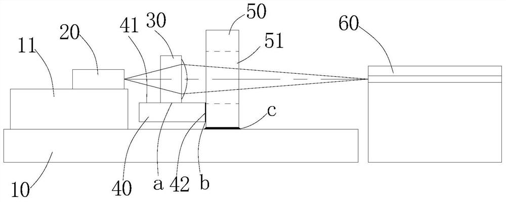
[0079] Such as image 3 In the illustrated embodiment 2, the optical assembly in this embodiment also includes a light emitting end. The difference from embodiment 1 is that in this embodiment, the connection surface 41 of the auxiliary part 40 is facing away from the substrate 10, and the lens element 30 is located on the auxiliary part 40 Above; the bonded position of the support member 50 and the auxiliary member 40 is below the light-transmitting surface or the light-through hole 51 , and other structures are consistent with Embodiment 1. When assembling, it is necessary to use a clamp to clamp the auxiliary part 40 from both sides of the auxiliary part 40 under the lens element 30. Also, the auxiliary part 40 is still not bonded to the substrate by bonding the bonding surface 42 of the auxiliary part 40 to the side of the support part 50. 10 contacts, avoiding the problem that the lens position may deviate due to temperature changes or moisture absorption due to too thick...

Embodiment 3

[0081] Such as Figure 4 The illustrated embodiment 3 is different from the embodiment 1 in that in this embodiment, the connection surface 41 of the auxiliary component 40 is perpendicular to the substrate 10 , and the lens element 30 is located on the side of the auxiliary component 40 . The bonding of the auxiliary part 40 and the support part 50 can be as Figure 5 and 6 Two bonding methods are shown.

[0082] Such as Figure 5 According to the bonding method, the bonding surface 42 of the auxiliary part 40 is still perpendicular to its connecting surface 41, and the side where the supporting part 50 and the auxiliary part 40 are bonded is on the same plane as the side where the light-transmitting surface or the light-passing hole 51 is located, and is located in the through-hole. The light surface or the side of the light hole 51 . The figure only shows that the bonding position of the auxiliary part 40 and the supporting part 50 is on one side of the light-transmitti...


PUM


Abstract

The present application discloses an optical component and a manufacturing method thereof. The component includes a substrate, a light-emitting element and a lens element arranged on the substrate according to an optical path, and a support and an auxiliary component; wherein the support includes a bottom surface connected to the substrate, And the side that is connected with the auxiliary part; the auxiliary part includes the connection surface connected with the lens element, and the bonding surface connected with the side of the support part; the bottom surface of the support part is bonded on the substrate, so that the bottom surface of the auxiliary part and the lens element The bottom surfaces are all higher than the upper surface of the substrate. The use of auxiliary parts that are pre-fixed or integrally formed with the lens is convenient for adjusting the position of the lens by clamping the auxiliary parts during assembly, which solves the problem of difficult lens clamping, and can adjust the position of the lens from three dimensions to achieve accurate coupling Or collimation, and it is easy to control the thickness of the glue layer within a small range, avoiding the problem that the glue layer is too thick to easily cause the lens position to deviate due to temperature changes or moisture absorption.

Description

technical field [0001] The present application relates to the technical field of optical communication, and in particular to an optical component including a lens element and a manufacturing method thereof. Background technique [0002] In the field of optical communication, especially in optical modules, it is indispensable to use lens elements to focus, couple or collimate optical signals. When the existing technical solutions are aimed at large-magnification lens coupling or collimating lens collimation, they are generally used with TEC (thermoelectric cooler) as a temperature control platform. When in use, the semiconductor laser, large magnification lens or collimating lens and receiving components (PIC, PLC, optical fiber or other optical waveguide devices) are all placed on the thermoelectric cooler and hermetically sealed. Because the epoxy resin used to fix the large magnification lens or collimating lens has a relatively high thermal expansion coefficient, and is ...

Claims


Application Information

Patent Timeline
Patent Type & Authority Patents(China)
IPC IPC(8): G02B6/27G02B6/293G02B6/32G02B6/42G02B7/02
CPCG02B6/4206G02B6/4239G02B6/4208G02B6/4215G02B6/4296G02B6/4244G02B6/4204H04B10/25891H04J14/02
Inventor 陈龙
Owner INNOLIGHT TECHNOLOGY (SUZHOU) LTD
Why Eureka
Try Eureka