Anisotropic conductive tape and preparation method thereof

A technology of anisotropic conduction and manufacturing method, which is applied in the direction of conductive adhesive, printed circuit manufacturing, circuit, etc., can solve the problems of increasing bump area and affecting the realization of driving lines, and achieve the design of multiple driving lines and improve the resolution rate effect

Active Publication Date: 2019-04-16
WUHAN CHINA STAR OPTOELECTRONICS SEMICON DISPLAY TECH CO LTD
View PDF8 Cites 2 Cited by
  • Summary
  • Abstract
  • Description
  • Claims
  • Application Information

AI Technical Summary

Problems solved by technology

The low density of conductive particles limits the number of conductive particles distributed in each bump, and if figure 1 As shown, the conductive particles in the existing ACF are randomly distributed, so in order for each bump to capture a certain number of conductive particles, the area of ​​the bump must be increased accordingly, which affects the realization of more driving circuit designs

Method used


Image

  • Anisotropic conductive tape and preparation method thereof
  • Anisotropic conductive tape and preparation method thereof
  • Anisotropic conductive tape and preparation method thereof

Examples


no. 1 example

[0059] Such as Figure 8 As shown, based on the above-mentioned anisotropic conductive tape, the present invention also provides a method for making an anisotropic conductive tape. The first embodiment of the method for making an anisotropic conductive tape of the present invention specifically includes the following steps:

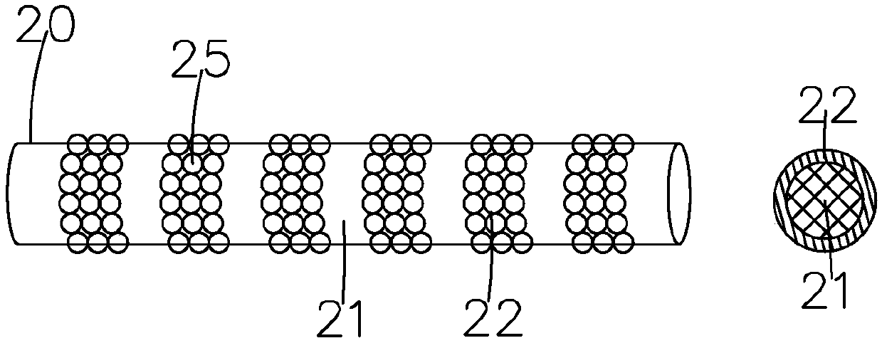
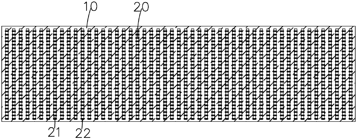
[0060] Step S1 , making a plurality of composite fibers 20 , and periodically arranging the plurality of composite fibers 20 .

[0061] Wherein, each composite fiber 20 includes an electrically insulating fiber 21 and a plurality of conductive rings 22 that are periodically arranged along the axial direction of the electrically insulating fiber 21 and are wrapped around the electrically insulating fiber 21; A plurality of conductive particles 25 adsorbed and co-encircled on the electrically insulating fibers.

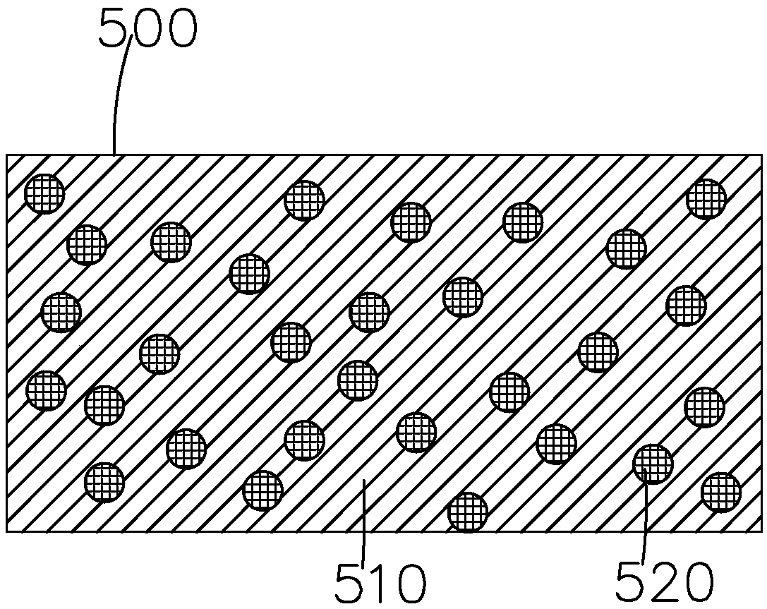
[0062] Specifically, the shape of the conductive particles 25 may be other shapes such as spherical, cubic, or conical.

[0063] Specifically, t...


PUM

PropertyMeasurementUnit
thicknessaaaaaaaaaa
lengthaaaaaaaaaa
widthaaaaaaaaaa

Abstract

The invention provides anisotropic conductive tape and a preparation method thereof. The anisotropic conductive tape comprises a resin baseband and multiple pieces of composite fibers arranged transversely in the resin baseband, each piece of the composite fiber comprises electrical insulating fiber and multiple conductive rings annularly sleeving the electrical insulating fiber, each conductive ring comprises multiple conductive particles jointly surrounding the corresponding electrical insulating fiber through adsorption, wherein multiple pieces of the composite fiber are arranged periodically in the resin baseband in the extending direction of the resin baseband, the conductive rings on each piece of the composite fiber are arranged periodically in the axial direction of the corresponding electrical insulating fiber of the composite fiber, because the conductive rings are fixed on the surface of the corresponding electrical insulating fiber, the conductive rings and the electrical insulating fiber are all not easily squeezed out of an electrode bump region during bonding, even if when the area of electrode bumps is reduced, the electrode bumps can still be in good contact with the conductive rings, thereby being capable of achieving the design of more driving circuits on a display panel, and being capable of effectively increasing the resolution ratio of the display panel.

Description

technical field [0001] The invention relates to the field of display technology, in particular to an anisotropic conductive adhesive tape and a manufacturing method thereof. Background technique [0002] Existing flat panel display devices on the market include liquid crystal display devices (Liquid Crystal Display, LCD) and active-matrix organic light emitting diode (Active-matrix organic light emitting diode, AMOLED) display devices. Among them, AMOLED has the characteristics of self-illumination, high brightness, wide viewing angle, high contrast, flexibility, low energy consumption, etc., so it has received widespread attention, and as a new generation of display methods, it has gradually replaced traditional liquid crystal displays and is widely used in Mobile phone screens, computer monitors, full-color TVs, etc. [0003] Existing flat-panel displays generally include a display panel (Panel) and an external circuit. When the display panel is normally displayed, an ext...

Claims


Application Information

Patent Timeline
Patent Type & Authority Applications(China)
IPC IPC(8): C09J7/22
CPCC09J7/22H01B3/48H01L2224/83851H01L24/29H01L24/27H01L2224/83101H01L2224/271H01L2924/12044H01L2224/29083H01L2224/29499H01L2224/13013H01L2224/14131H01L2224/81193H01L2224/81903H01L24/81H01L24/83H01L24/13H01L24/14H01L2224/9211H01L24/92H01L2224/2929H01L2224/29386H01L2224/2939H01L2224/294H01L2224/29186H01L2224/2919H05K3/323H05K2201/10128G02F1/13452H01L2924/00012H01L2224/81H01L2224/83H01L2924/00014C09J2301/314C09J2301/50C09J2301/408C09J9/02C09J2203/326
Inventor 杨汉宁
Owner WUHAN CHINA STAR OPTOELECTRONICS SEMICON DISPLAY TECH CO LTD
Why Eureka
Try Eureka