Display panel and manufacturing method thereof

A manufacturing method and display panel technology, applied in semiconductor/solid-state device manufacturing, optics, instruments, etc., can solve problems such as electrostatic discharge of display panels, and achieve the effect of improving yield and quality

Active Publication Date: 2019-04-19
SHENZHEN CHINA STAR OPTOELECTRONICS SEMICON DISPLAY TECH CO LTD
View PDF1 Cites 3 Cited by
  • Summary
  • Abstract
  • Description
  • Claims
  • Application Information

AI Technical Summary

Problems solved by technology

[0005] This application provides a display panel and its manufacturing method to solve the technical

Method used


Image

  • Display panel and manufacturing method thereof
  • Display panel and manufacturing method thereof
  • Display panel and manufacturing method thereof

Examples


Example Embodiment

[0038] The following descriptions of the various embodiments refer to the accompanying drawings to illustrate specific embodiments that the present application can be used to implement. The directional terms mentioned in this application, such as [top], [bottom], [front], [back], [left], [right], [inside], [outside], [side], etc., are for reference only The orientation of the attached schema. Therefore, the directional terms used are used to illustrate and understand the application, but not to limit the application. In the figures, structurally similar elements are denoted by the same reference numerals.

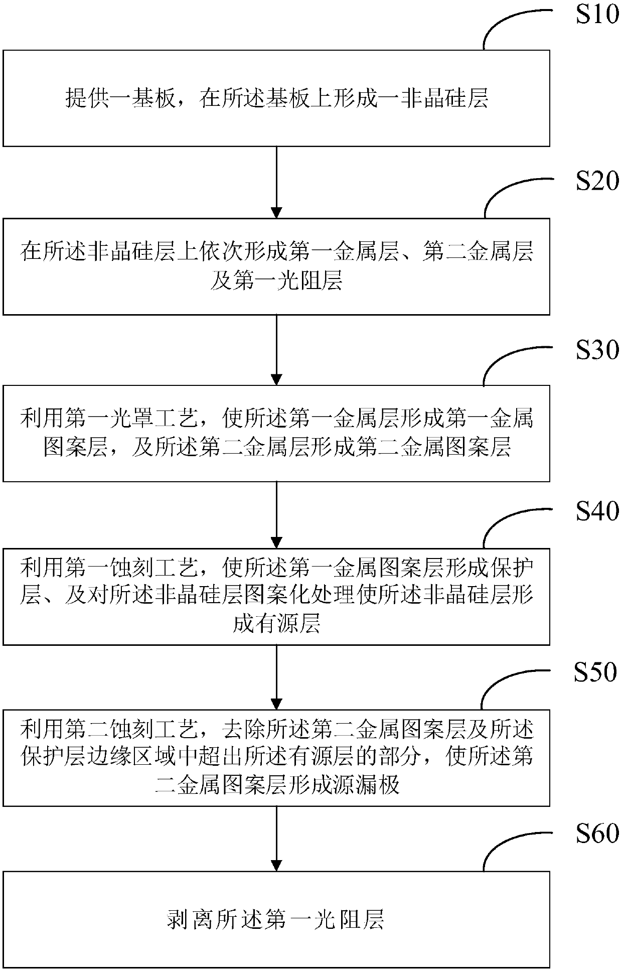
[0039] see figure 1 , figure 1 It is a step diagram of a method for manufacturing a display panel of the present application.

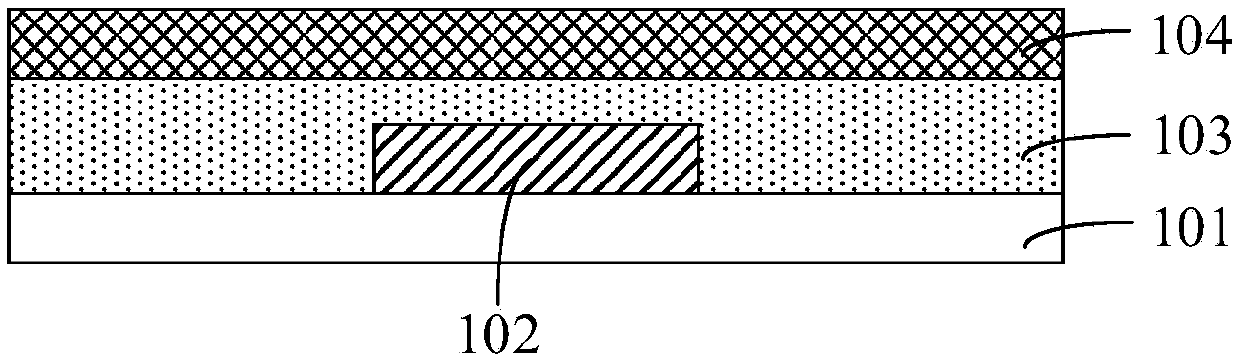
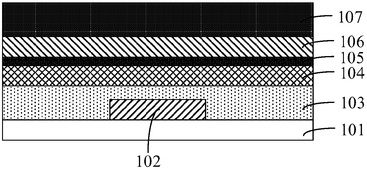
[0040] see Figure 2A-2F , Figure 2A-2F It is a process diagram of a method for manufacturing a display panel of the present application.

[0041] Described preparation method comprises:

[0042] S10, providing a substrate, and forming an ...


PUM


Abstract

The invention provides a display panel and a manufacturing method thereof. The manufacturing method of the display panel comprises the steps of: providing a substrate, wherein an amorphous silicon layer, a first metal layer, a second metal layer, and a first photoresist layer are sequentially formed on the substrate; utilizing a first mask process, thus the first metal layer forms a first metal pattern layer, and the second metal layer forms a second metal pattern layer; utilizing a first etching process to make the first metal pattern layer form a protective layer, and performing patterning processing on the amorphous silicon layer so that the amorphous silicon layer forms an active layer; and utilizing a second etching process to remove portions exceeding the active layer in edge regionsof the second metal pattern layer and the protective layer, so that the second metal pattern layer forms a source and a drain. Through forming the protective layer between the active layer and the source and the drain, the active layer under the source and the drain is avoided from being etched when performing patterning processing on the source and the drain, thereby improving the yield and quality of the product.

Description

technical field [0001] The present application relates to the display field, in particular to a display panel and a manufacturing method thereof. Background technique [0002] LCD (Liquid Crystal Display, liquid crystal display) is the most widely used display product in the market at present. Its production technology is very mature, the product yield rate is high, the production cost is relatively low, and the market acceptance is high. [0003] In the existing LCD manufacturing process, a source-drain metal layer is disposed on the active layer. Due to the ashing process, the photoresist layer on the source-drain metal layer becomes thinner, and part of the source-drain metal layer is exposed. Therefore, when the source-drain metal layer is etched, part of the active layer below the source-drain metal layer will be etched away at the same time, resulting in the risk of electrostatic discharge of the product and reducing the yield of the product. [0004] Therefore, the ...

Claims


Application Information

Patent Timeline
IPC IPC(8): H01L21/84H01L21/336H01L27/12H01L29/786G02F1/136
CPCG02F1/136G02F1/136295H01L27/1222H01L27/127H01L29/66765H01L29/78606H01L29/78669
Inventor 袁文豪
Owner SHENZHEN CHINA STAR OPTOELECTRONICS SEMICON DISPLAY TECH CO LTD
Why Eureka
Try Eureka