Back surface structure of IGBT chip, IGBT chip structure and preparation method thereof

A backside structure and chip technology, which is applied in semiconductor/solid-state device manufacturing, electrical components, transistors, etc., can solve the problems of current concentration process manufacturing cost in the transition zone, avoid local over-temperature or over-current failure, and save photolithography Process, the effect of improving reliability

Active Publication Date: 2019-04-23
GLOBAL ENERGY INTERCONNECTION RES INST CO LTD +2
View PDF5 Cites 6 Cited by
  • Summary
  • Abstract
  • Description
  • Claims
  • Application Information

AI Technical Summary

Problems solved by technology

[0003] Therefore, the present invention provides a back structure of an IGBT chip, an IGBT chip structure and a preparation method thereof, which overcome the defect of high manufacturing cost of the process used in the prior art to solve the problem of current concentration in the transition region

Method used


Image

  • Back surface structure of IGBT chip, IGBT chip structure and preparation method thereof
  • Back surface structure of IGBT chip, IGBT chip structure and preparation method thereof
  • Back surface structure of IGBT chip, IGBT chip structure and preparation method thereof

Examples


Embodiment 1

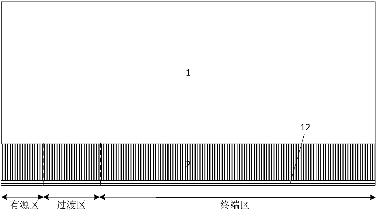
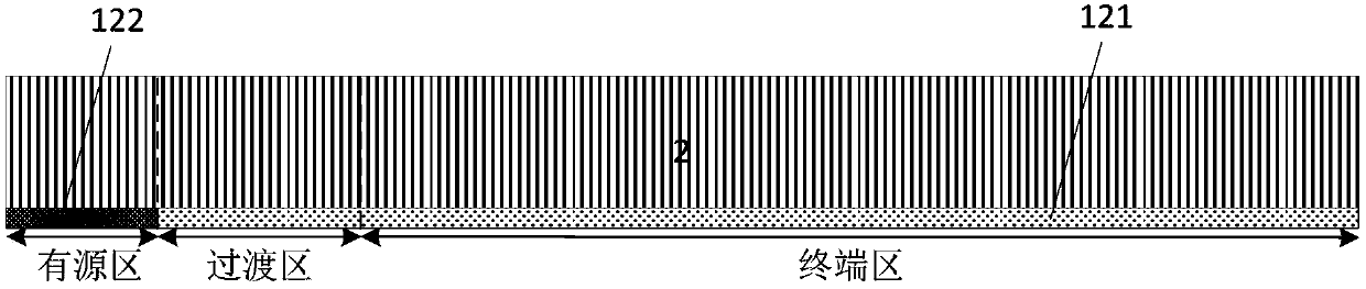
[0047] An embodiment of the present invention provides a backside structure of an IGBT chip, including: a buffer layer 2 and a doped layer 12, wherein the doped layer 12 is formed by ion implantation at a first preset depth of the buffer layer 2; The doped layer in the terminal region and the transition region of 2 is subjected to the first preset high temperature annealing treatment; the doped layer located in the active region of the buffer layer 2 is subjected to the first preset high temperature annealing treatment and the second preset high temperature annealing treatment. The first preset high-temperature annealing treatment is furnace tube annealing treatment, the annealing temperature is 350-500°C, and the annealing time is 30-120min; the second preset high-temperature annealing treatment is laser annealing treatment, the laser wavelength is 500nm-700nm, and the laser energy is 0.8J-4.0 J, the above is just an example, not a limitation.

[0048] In the embodiment of th...

Embodiment 2

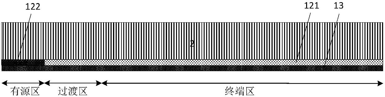
[0054] The back structure of the IGBT chip provided by the embodiment of the present invention, such as Figure 4 As shown, the back structure of the IGBT chip includes: a buffer layer 2, a doped layer 3 and a defect layer 11, wherein the structure and manufacturing process of the buffer layer 2 and the doped layer 3 are the same as those of the back side of the IGBT chip in Example 1. The structure of the buffer layer 2 and the doped layer 3 is the same, and will not be repeated here. The defect layer 11 is formed by performing ion implantation at a second predetermined depth of the buffer layer, the second predetermined depth is greater than the above-mentioned first predetermined depth, and the defect layer 11 penetrates the active region, the transition region and the terminal of the buffer layer 2 Area. In one embodiment, the defect layer 11 is formed by implanting inert ions into the buffer layer, specifically, the inert ions can be argon ions, and the implantation dose...

Embodiment 3

[0058] An embodiment of the present invention provides an IGBT chip structure, including: the front structure of the IGBT chip and the back structure of the IGBT chip described in Embodiment 1 or Embodiment 2. The IGBT front-side process is carried out on the substrate 1 made of silicon material. The front-side structure includes: a voltage-resistant field ring 31 in the terminal area, a polysilicon field plate 7, a metal field plate 81, a stop ring 41 and a passivation layer 10. The active area is light Doping P-type 3 and heavily doping P-type 4, N-type emitter 5, gate oxide layer 6, polysilicon field plate 7, oxide layer 9 and active region metal layer 8, forming a structure such as Image 6 Shown is just an example, not a limitation.

[0059] The IGBT chip structure provided by the embodiment of the present invention can not only realize different hole injection efficiencies between the collector active region and the terminal region on the back of the IGBT, improve the cu...


PUM


Abstract

The invention discloses a back surface structure of an IGBT chip, an IGBT chip structure and a preparation method thereof. The back surface structure comprises: a buffer layer and a doped layer, the doped layer is formed by ion implantation in the buffer layer; the doped layer of a terminal region and a transition region is subjected to high-temperature annealing treatment; a doped layer of the active region is subjected to twice high-temperature annealing treatment to achieve different hole injection efficiencies of the active region and the terminal region so as to improve the current concentration problem in the IGBT transition region and improve the reliability. Compared to the prior art of a treatment mode that a photolithography process is used to implant different doses of doping ions on the back side of the active region and the terminal region to achieve different injection efficiencies of the back surface collectors of the active region and the terminal region, the back surface structure of the IGBT chip, the IGBT chip structure and the preparation method thereof only employ the annealing process to omit the photolithography process so as to save the manufacturing cost. An inert ion defect layer is implanted in the buffer layer to form a defect layer, so that the IGBT back surface collector can adopt a higher doping concentration, and the IGBT back surface and the back surface metal easily form good ohmic contact, thereby reducing the IGBT on-state voltage drop.

Description

technical field [0001] The invention relates to the technical field of power electronic devices, in particular to a backside structure of an IGBT chip, an IGBT chip structure and a preparation method. Background technique [0002] With the continuous development of power electronic technology, the switching frequency and performance requirements of various main switching devices have been continuously improved, which has put forward higher requirements for IGBT performance and reliability. Generally, the transition area of ​​IGBT chips has the problem of current concentration during the turn-off process. , that is, the holes injected from the back collector to the terminal when the IGBT is turned on, are mainly extracted from the PN junction in the transition region of the IGBT chip during the turn-off process, resulting in current concentration in the transition region. In order to alleviate the problem of current concentration in the transition region, the injection effici...

Claims


Application Information

Patent Timeline
Patent Type & Authority Applications(China)
IPC IPC(8): H01L29/739H01L21/265H01L29/06H01L29/40H01L21/331
CPCH01L29/0638H01L29/404H01L29/66333H01L29/7398H01L21/26513
Inventor 曹功勋朱涛刘瑞吴昊金锐吴军民潘艳
Owner GLOBAL ENERGY INTERCONNECTION RES INST CO LTD
Why Eureka
Try Eureka