

Broadband high-gain circularly polarized microstrip antenna
A microstrip antenna and high-gain technology, which is applied to antenna grounding devices, antenna arrays that are powered independently, and antenna grounding switch structural connections, etc., can solve the problem of increasing antenna feed loss, increasing processing complexity, and increasing antenna size, etc. problem, to achieve the effect of wide axial ratio bandwidth, reduce lateral leakage, and reduce feed loss
- Summary
- Abstract
- Description
- Claims
- Application Information
AI Technical Summary
Problems solved by technology
Method used
Image

Examples
Embodiment Construction
[0027] The present invention will be further described below in conjunction with accompanying drawing.
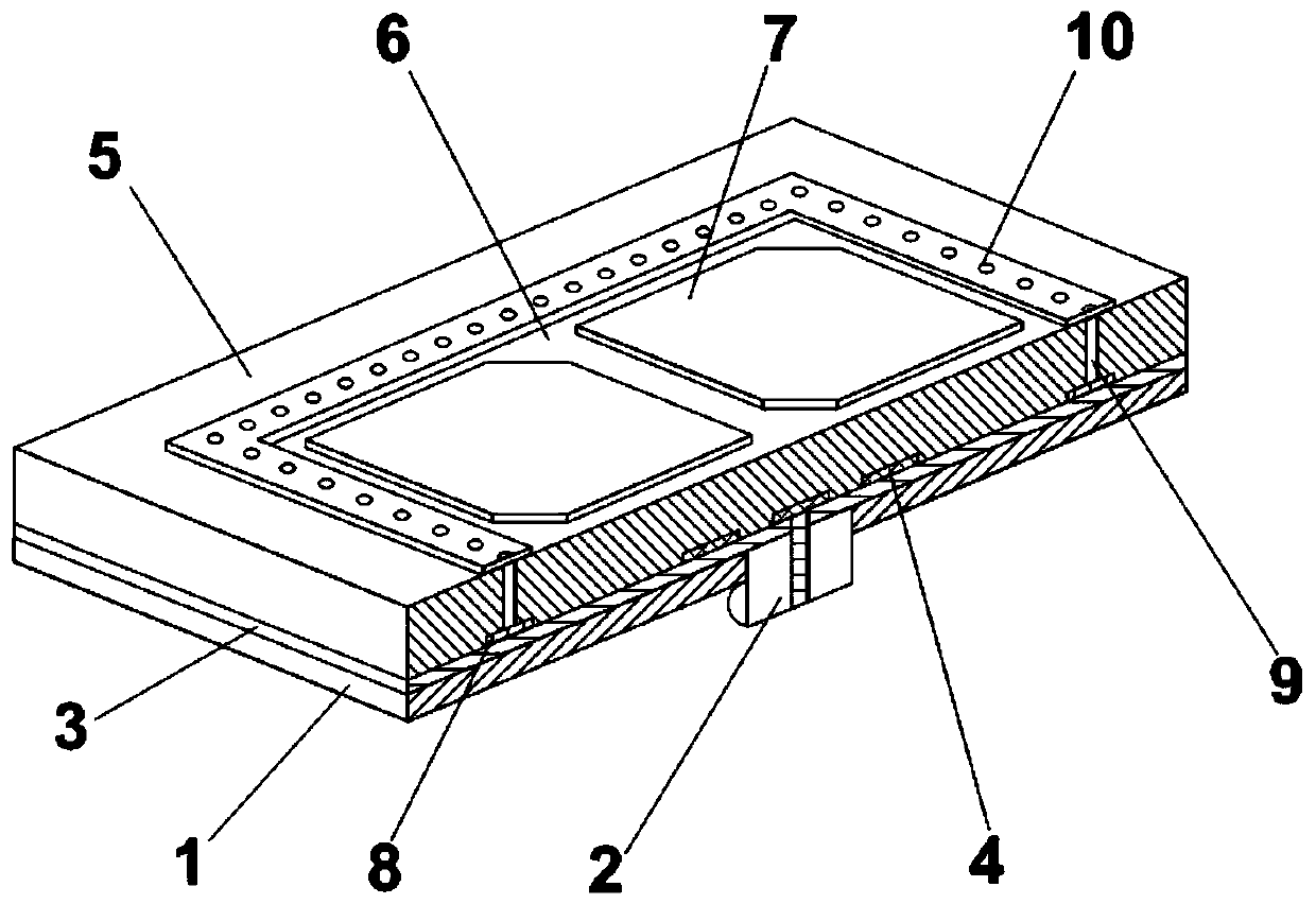
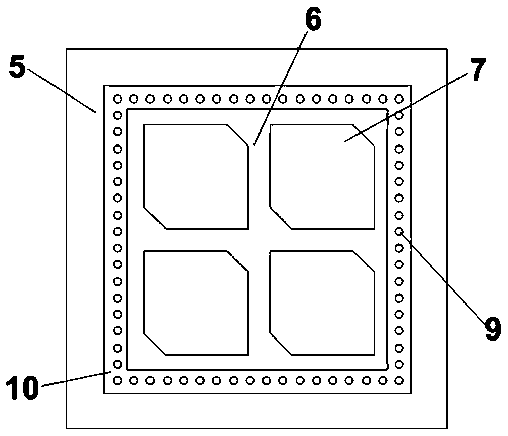
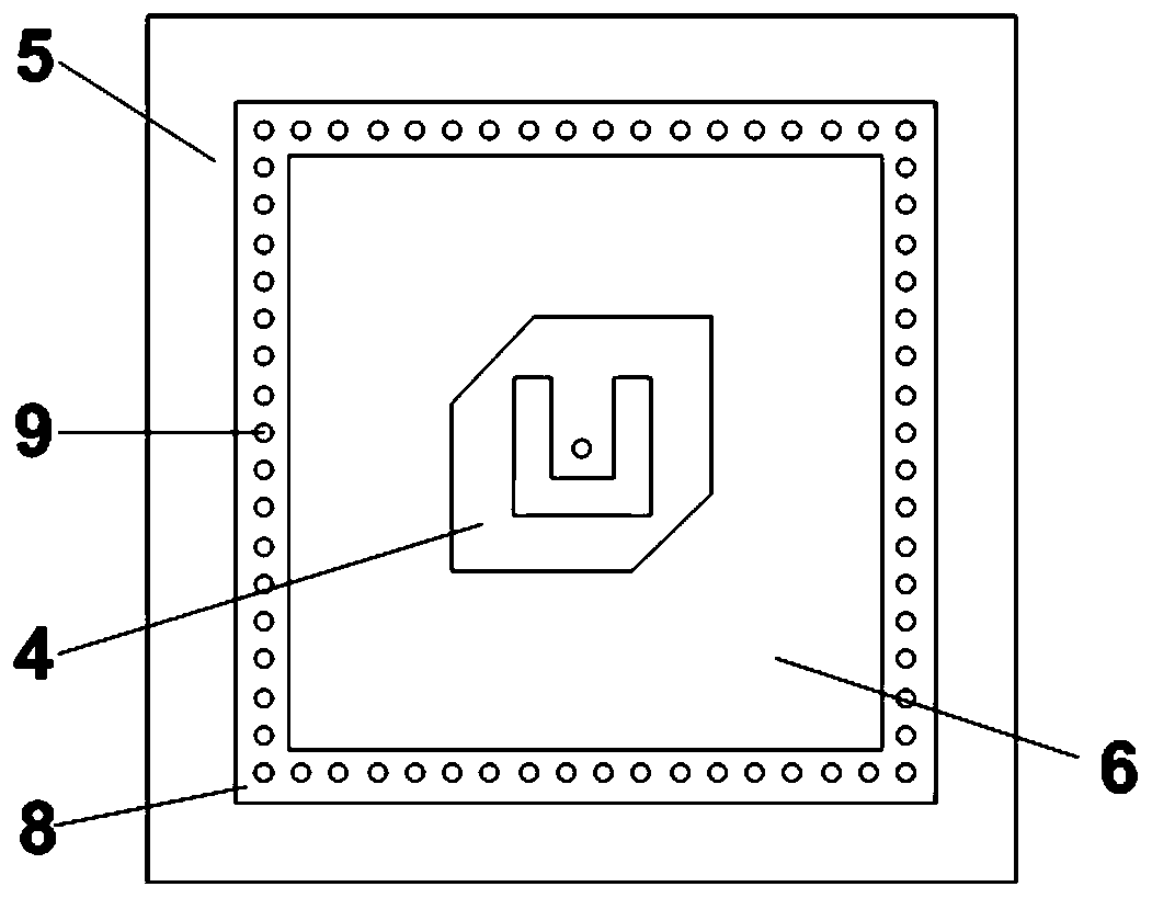
[0028] figure 1 Shown is the schematic diagram of the layered structure of the antenna of the present invention, as can be seen from the figure, the wide-band high-gain circularly polarized microstrip antenna proposed by the present invention includes: floor 1, feed coaxial 2, bottom dielectric substrate 3, cut corner U-shaped groove microstrip 4, top layer dielectric substrate 5, substrate integrated waveguide square cavity 6, microstrip radiation unit 7; the microstrip antenna of the present invention can be processed by common double-layer microstrip printed board technology, and can also be processed by LTCC Craft realized.
[0029] Among them, the structural floor (1) is located at the bottom of the antenna and is made of metal, the bottom dielectric substrate 3 is located on the upper layer of the floor 1 and is in close contact, the top dielectric substrate 5 is loc...
PUM
 Abstract
Description
Claims
Application Information