Silicon-base nano-antenna with unidirectional radiation characteristic

A radiation characteristic and nano-antenna technology, applied in the field of optical phased array, can solve problems such as energy waste, energy leakage, and low efficiency, and achieve the effect of realizing one-way radiation, suppressing leakage, and improving efficiency

Inactive Publication Date: 2019-05-03
UNIV OF ELECTRONICS SCI & TECH OF CHINA
View PDF3 Cites 0 Cited by
  • Summary
  • Abstract
  • Description
  • Claims
  • Application Information

AI Technical Summary

Problems solved by technology

However, at present, antennas on silicon substrates suffer from energy leakage toward the substrate side and low efficiency.
This is due to the structural characteristics of SOI itself (ie: silicon substrate-silicon dioxide insulating layer-silicon device layer, stacked structure), because light always tends to propagate in a medium with a high dielectric constant, and the lower layer The dielectric constant of the silicon substrate and the silicon dioxide insulating layer are higher than that of free space, so that a large part of the radiation of the antenna located on the silicon device layer will leak toward the substrate side instead of radiating into the free space, which makes at least some half the energy wasted
At the same time, due to the limitations of the SOI process, it is impossible to add a metal reflector directly under the device layer to achieve unidirectional radiation.

Method used


Image

  • Silicon-base nano-antenna with unidirectional radiation characteristic
  • Silicon-base nano-antenna with unidirectional radiation characteristic
  • Silicon-base nano-antenna with unidirectional radiation characteristic

Examples


Embodiment 1

[0016] Embodiment 1 Nano patch linear array design

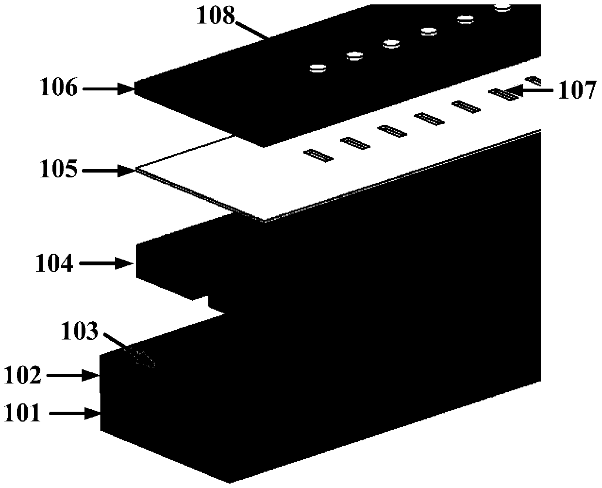
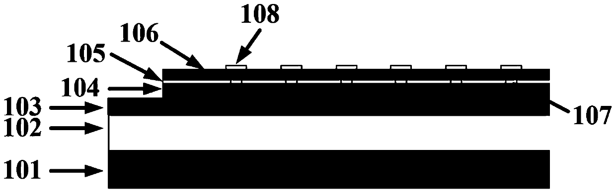
[0017] The nano-patch array on the silicon substrate based on the gap coupling of this embodiment adopts a linear array form, such as figure 1 shown. The bottom silicon layer 101, the silicon dioxide layer 102, and the strip silicon waveguide 103 together constitute a typical SOI structure, and the silicon waveguide is covered with a silicon dioxide cladding layer 104. The upper side of the silicon dioxide coating is a metal film 105, and a small hole array 106 is etched on the metal film. The topmost layer is the nano patch array 108, and there is a silicon dioxide thin layer 106 support between the nano patch array 108 and the metal film 105. figure 2 shown as figure 1 A cutaway view of the center of the antenna. The width and height of the strip silicon waveguide 103 are 460 nm and 240 nm, respectively. The thickness of the silver thin film 105 is 80 nm, and the length and width of the nanometer holes 106 on the sil...

Embodiment 2

[0020] Embodiment 2 nano-patch optical phased array design

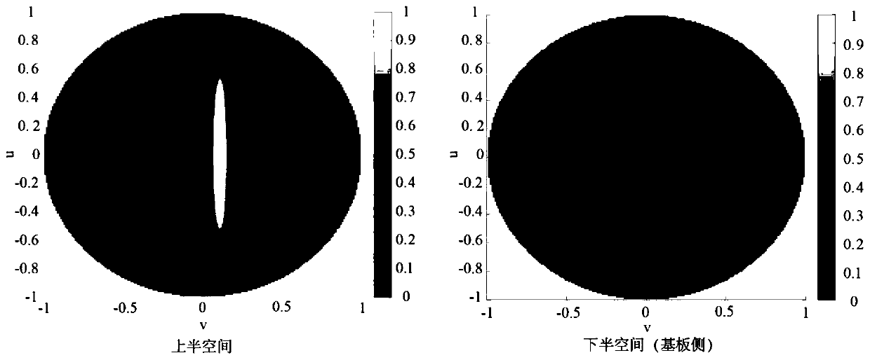
[0021] Specifically, the linear array in Embodiment 1 is extended perpendicular to the feeding direction to form a two-dimensional array. Beam scanning can be realized by changing the feed phase of each linear array. Its size parameter is the same as that of Example 1, and the distance between channels is 0.9 μm. Image 6 The beam scanning pattern of the optical phased array in this example under different phase differences between channels is given. It can be seen that with the proposed antenna, beam scanning without grating lobe of ±45° can be achieved. And in the whole scanning range, there is no obvious back lobe, indicating that the leakage on the substrate side is effectively suppressed.


PUM


Abstract

The invention discloses a silicon-base nano-antenna with a unidirectional radiation characteristic and belongs to the technical field of optical phased array and laser radar, in particular to a silicon-base nano-antenna array with a unidirectional radiation characteristic, and in particular to a high-efficiency and high-directionality silicon-base nano-antenna arrays for laser imaging, laser radarand optical communication systems. The energy is coupled from a silicon dielectric waveguide by using small holes on a metal film. The asymmetry is introduced by the strong resonance characteristic of a nano patch antenna, thereby realizing the unidirectional radiation of the antenna on a silicon substrate, suppressing leakage to a substrate side, and improving the efficiency of the antenna.

Description

technical field [0001] The invention belongs to the technical field of optical phased array and laser radar, and specifically relates to a silicon-based nano-antenna array with unidirectional radiation characteristics, in particular to a silicon-based nano-antenna array with high efficiency and high orientation, which is suitable for laser imaging and laser radar and optical communication systems. Background technique [0002] As a key technology for laser imaging, detection and ranging, optical phased arrays have important applications in autonomous driving, remote sensing mapping and military fields. The traditional optical phased array uses a mechanical method to realize beam scanning. Due to the inherent low speed and other defects of the mechanical method itself, it can no longer meet the requirements of modern high-performance lidar systems. In recent years, due to the advancement of micro-nano processing technology and the development of integrated optical technology...

Claims


Application Information

Patent Timeline
Patent Type & Authority Applications(China)
IPC IPC(8): H01Q21/00H01Q1/36
Inventor 屈世伟曾元松
Owner UNIV OF ELECTRONICS SCI & TECH OF CHINA
Why Eureka
Try Eureka