SiC high-temperature pressure sensor without lead package and manufacturing method thereof

A technology of a pressure sensor and a manufacturing method, which is applied in the field of wide-bandgap semiconductor device preparation, can solve the problems of narrow bandgap width, degradation of mechanical properties of silicon materials, poor high temperature resistance and radiation resistance, etc.

Inactive Publication Date: 2019-05-07
WUHAN UNIV
View PDF8 Cites 14 Cited by
  • Summary
  • Abstract
  • Description
  • Claims
  • Application Information

AI Technical Summary

Problems solved by technology

Therefore, the following reasons limit the application of silicon-based sensors under high temperature and harsh conditions: 1. Due to the narrow band gap of silicon materials, their high temperature resistance and radiation resistance are poor; 2. Silicon materials are easy to interact with the medium Chemical reaction, oxidation or corrosion; 3. Silicon materials are prone to mechanical degradation under high temperature conditions

Method used


Image

  • SiC high-temperature pressure sensor without lead package and manufacturing method thereof
  • SiC high-temperature pressure sensor without lead package and manufacturing method thereof
  • SiC high-temperature pressure sensor without lead package and manufacturing method thereof

Examples


Embodiment Construction

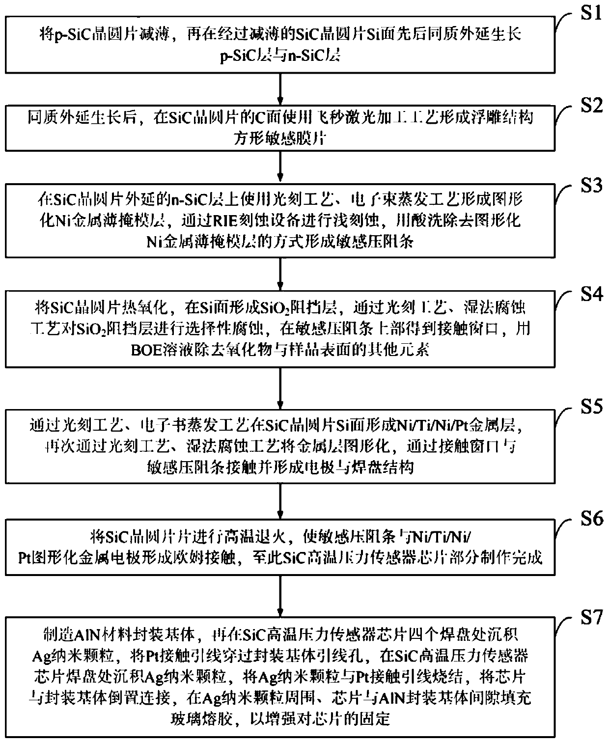
[0050] The specific embodiments of the leadless packaged SiC high-temperature pressure sensor and its manufacturing method involved in the present invention will be described in detail below with reference to the accompanying drawings.

[0051]

[0052] Such as figure 1 As shown, the method for manufacturing a leadless packaged SiC high-temperature pressure sensor provided in this embodiment includes the following steps:

[0053] (1) if figure 2 and 3 As shown, the p-SiC wafer 100 is thinned to 130 μm, image 3 The dashed line shows the thinned part; as Figure 4 As shown, the Si surface of the thinned SiC wafer 100 is homoepitaxially grown with a thickness of 5 μm and a doping concentration of 3×10 18 cm -3(±15%) p-SiC layer 101, the growth thickness is 2 μm, and the doping concentration is 1×10 19 cm -3 (±15%) n-SiC layer 102 .

[0054] (2) if Figure 5-7 As shown, a square sensitive diaphragm 103 with a relief structure is formed on the C surface of the p-SiC wa...


PUM

PropertyMeasurementUnit
thicknessaaaaaaaaaa
diameteraaaaaaaaaa
thicknessaaaaaaaaaa

Abstract

The invention provides a SiC high-temperature pressure sensor without lead package and a manufacturing method thereof. The manufacturing method comprises the steps: a p-SiC wafer sheet is thinned, anda p-SiC layer and an n-SiC layer are sequentially grown on the Si surface; a sensitive membrane of a square emboss structure is formed on the C surface; an imaging masking layer is formed on the n-SiC layer, and shallow etching and acid pickling are conducted to form a sensitive pressure resistance strip; a blocking layer is formed on the Si surface through thermal oxidation and selectively corroded, and a contact window is obtained in the upper part of the sensitive pressure resistance strip; an Ni/Ti/Ni/Ni/Pt metal layer is formed on the Si surface and imaged, and makes contact with the sensitive pressure resistance strip through the contact window to form an electrode and a bonding pad; high-temperature annealing is conducted to enable the sensitive pressure resistance strip and the metal electrode to form Ohm contact to form a static pressure compensation unit; and a package base body is manufactured, Ag nanoparticles are deposited at the chip bonding pad, a Pt lead penetrates through a lead hole to be sintered with the Ag nanoparticles, and then gaps are filled with glass collosol.

Description

technical field [0001] The invention belongs to the technical field of preparation of wide bandgap semiconductor devices, and in particular relates to a leadless packaged SiC high-temperature pressure sensor and a manufacturing method thereof. technical background [0002] Sensor technology is an important symbol of the development level of modern science and technology, and pressure sensors are the most widely used category. A pressure sensor is a semiconductor electronic component that can convert an analog signal such as pressure into an electrical signal. With the development of semiconductor technology and MEMS technology, people use silicon as the main material of pressure sensors, and adopt various forms such as capacitance and piezoresistive. , which is characterized by small size, light weight, high accuracy, and good temperature characteristics. As people's research on more extreme, especially high-temperature environments deepens, pressure sensors need to work in...

Claims


Application Information

Patent Timeline
Patent Type & Authority Applications(China)
IPC IPC(8): G01L1/18
Inventor 周圣军徐浩浩刘星童李宁
Owner WUHAN UNIV
Why Eureka
Try Eureka