Chip scale package LED light source and manufacturing method thereof
A chip-level packaging, LED light source technology, applied in electrical components, circuits, semiconductor devices, etc., can solve the problems of easy-to-break CSPLED chips, easy colloid fall off, weak mechanical strength of CSPLED, etc., to improve the anti-vulcanization ability and mechanical strength. , the effect of improving the anti-stress ability
- Summary
- Abstract
- Description
- Claims
- Application Information
AI Technical Summary
Problems solved by technology
Method used
Image

Examples
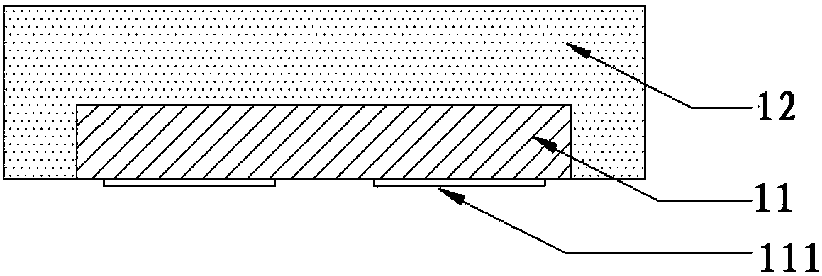
Embodiment 1
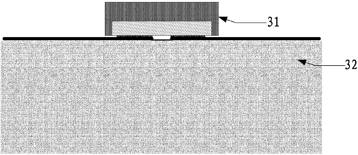
[0042] see image 3 As shown, the chip-scale package LED31 is fixed on the circuit board 32. Since the chip-scale package LED31 has no substrate, its mechanical strength is low. , the chip-scale package LED31 is easy to break and produce lack of brightness; meanwhile, the fluorescent glue or white wall glue around the chip in the chip-scale package LED31 is also easy to detach after high and low temperature cycles, resulting in a great change in the luminous color.
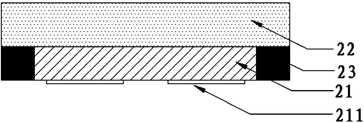
[0043] In order to solve the above problems, this embodiment provides a new chip-scale package LED light source. The chip-scale package LED light source provided by this embodiment can be used in various fields such as illumination, indication and backlight. see Figure 4 As shown, the chip-scale package LED light source provided in this embodiment includes a circuit board 42, a chip-scale package LED 41 fixed on the circuit board, and a protective adhesive layer 43 formed on the circuit board and covering the ch...
Embodiment 2
[0056] In order to better understand the present invention, this embodiment further describes the present invention by taking a manufacturing method of the chip-scale package LED light source shown in Embodiment 1 as an example.
[0057] See Figure 8 As shown, the chip-scale package LED light source manufacturing method provided in this embodiment includes:
[0058] S801: Fixing the chip scale package LED on the circuit board.
[0059] In this embodiment, the way of fixing the chip-scale package LED on the circuit board for electrical connection can be various ways to realize the electrical connection between the chip-scale package LED and the circuit board, for example including but not limited to welding, conductive bonding and so on.
[0060] In this embodiment, the number of chip-scale packaged LEDs fixed on the circuit board can be flexibly set according to specific application scenarios, and only one LED can be fixed, or multiple LEDs can be fixed.
[0061] In this em...
Embodiment 3
[0079] In order to better understand the present invention, this embodiment takes the chip-scale packaged LED light source as an example as a backlight light source, and combines a complete production process from preparation to storage to further illustrate the present invention. see Figure 11 As shown, the production process includes:
[0080] S1101: Fix the circuit board (eg PCB board) on the carrier.
[0081] S1102: Spray codes on the circuit board, this step can be omitted, and the specific content of the codes can be sprayed with the manufacturer's name, product name, performance parameters, logos, etc.
[0082] S1103: Print solder paste on the corresponding pads on the circuit board, and the specific printing method can be flexibly selected.
[0083] S1104: To perform solder paste printing inspection, SPI (Solder Paste Inspection) can be used for inspection, so as to detect whether the solder paste printing is offset, the height deviation of the solder paste printing...
PUM
 Abstract
Description
Claims
Application Information
 - R&D
- Intellectual Property
- Life Sciences
- Materials
- Tech Scout
- Unparalleled Data Quality
- Higher Quality Content
- 60% Fewer Hallucinations
Browse by: Latest US Patents, China's latest patents, Technical Efficacy Thesaurus, Application Domain, Technology Topic, Popular Technical Reports.
© 2025 PatSnap. All rights reserved.Legal|Privacy policy|Modern Slavery Act Transparency Statement|Sitemap|About US| Contact US: help@patsnap.com