Single photon source device, preparation method and quantum memory

A single-photon source and device technology, applied in the direction of static memory, digital memory information, information storage, etc., can solve the problems of small adjustment range of the central wavelength of the luminescence spectrum, unsatisfactory compact chip integration trend, and single adjustment direction. Achieve the effect of large wavelength adjustment range

Pending Publication Date: 2019-05-10
SHANGHAI INST OF MICROSYSTEM & INFORMATION TECH CHINESE ACAD OF SCI
View PDF3 Cites 4 Cited by
  • Summary
  • Abstract
  • Description
  • Claims
  • Application Information

AI Technical Summary

Problems solved by technology

[0007] In view of the above-mentioned shortcomings of the prior art, the purpose of the present invention is to provide a single photon source device, a preparation method and a quantum memory, which are used to solve the problem of th

Method used


Image

  • Single photon source device, preparation method and quantum memory
  • Single photon source device, preparation method and quantum memory
  • Single photon source device, preparation method and quantum memory

Examples


Embodiment 1

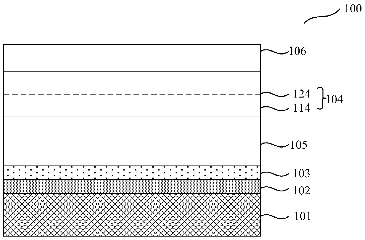
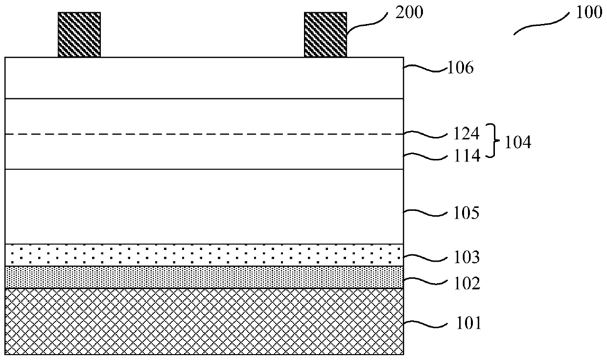
[0060] This embodiment provides a single photon source device, the single photon source device includes:

[0061] A quantum dot luminescent layer, the quantum dot luminescent layer includes a barrier layer and a quantum dot layer located in the barrier layer;

[0062] A piezoelectric ceramic substrate, through which the central wavelength of the emission spectrum of the quantum dot light-emitting layer is adjusted;

[0063] A bonding layer, the bonding layer is located between the quantum dot luminescent layer and the piezoelectric ceramic substrate, and the quantum dot luminescent layer and the piezoelectric ceramic substrate are connected through the bonding layer.

[0064] In this embodiment, the single photon source device has a piezoelectric ceramic substrate, so that the single photon source device has a large wavelength adjustment range, the wavelength can be adjusted bidirectionally, and the trend of compact on-chip integration can be met.

[0065] Specifically, such ...

Embodiment 2

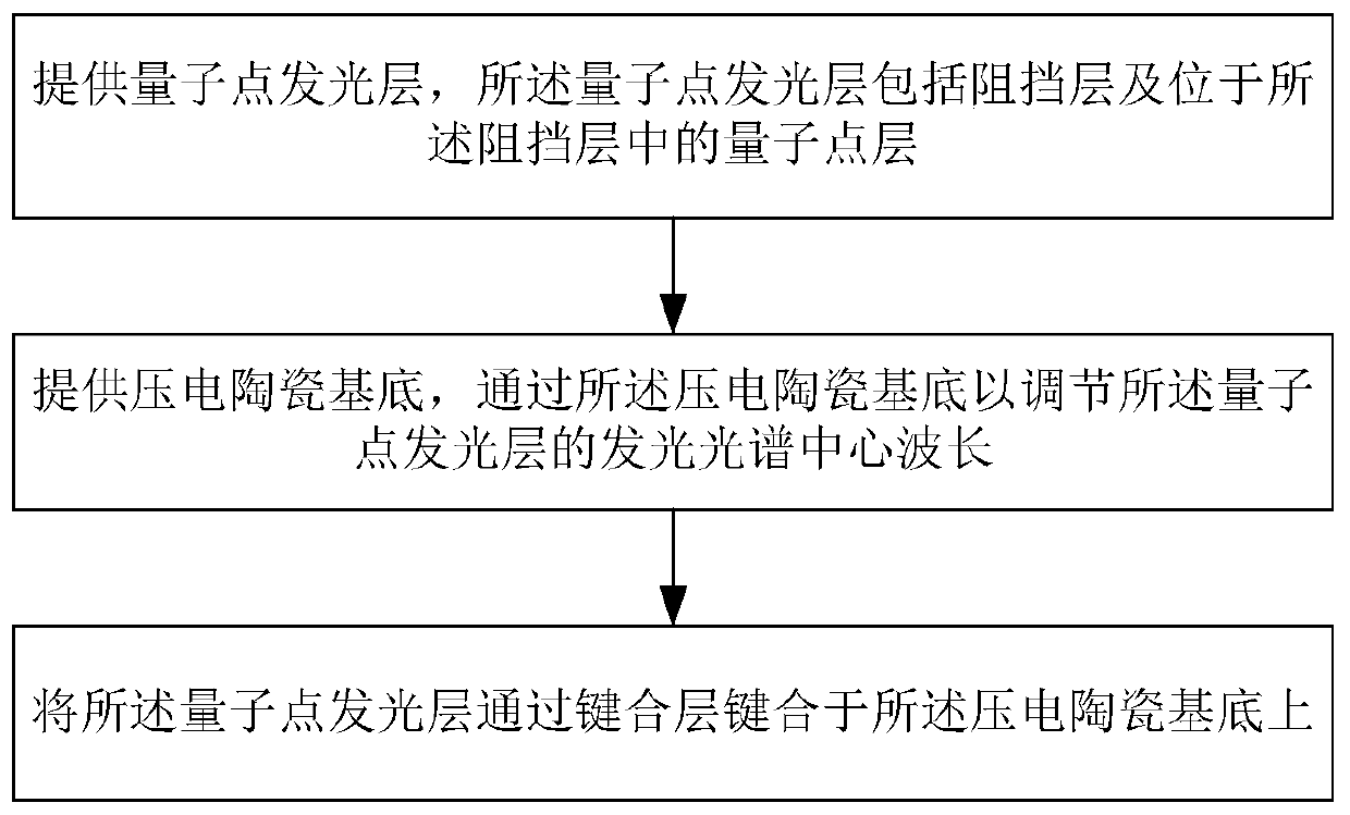
[0085] Such as figure 1 , this embodiment provides a method for preparing a single photon source device, which can be used to prepare any one of the above single photon source devices, but is not limited thereto. Specifically include the following steps:

[0086] A quantum dot luminescent layer is provided, the quantum dot luminescent layer includes a blocking layer and a quantum dot layer located in the blocking layer;

[0087] A piezoelectric ceramic substrate is provided, through which the central wavelength of the luminescent spectrum of the quantum dot luminescent layer is adjusted;

[0088] The quantum dot light-emitting layer is bonded on the piezoelectric ceramic substrate through a bonding layer.

[0089] This embodiment provides a method for preparing a single photon source device with a piezoelectric ceramic substrate, so that the quantum dot light-emitting layer on the piezoelectric ceramic substrate has a large wavelength adjustment range, the wavelength can be a...

Embodiment 3

[0110] This embodiment provides a test device for a single photon source device, the test device includes a 532nm neodymium-doped yttrium vanadate continuous light laser, through the 532nm neodymium-doped yttrium vanadate continuous light laser to any of the above-mentioned Single photon source devices were tested.

[0111] As a further embodiment of this embodiment, the test device includes a test device for testing one or a combination of photoluminescence of the single photon source device, wavelength shift under stress conditions, and single photon characteristics.

[0112] Such as Figure 10 , shown as a testing device for a single photon source device in this embodiment; Figure 11 to Figure 14 , showing the spectrum obtained by testing the single photon source device in this embodiment through the test device of the single photon source device.

[0113] Specifically, firstly make the Figure 8a The single photon source device in is placed in a cryostat, such as a liq...


PUM

PropertyMeasurementUnit
Thicknessaaaaaaaaaa
Thicknessaaaaaaaaaa
Thicknessaaaaaaaaaa

Abstract

The present invention provides a single photon source device, a preparation method and a quantum memory. The single photon source device comprises: a quantum dot luminescent layer, wherein the quantumdot luminescent layer comprises a barrier layer and a quantum dot layer in the barrier layer; a piezoelectric ceramic substrate, wherein the central wavelength of the luminescent spectrum of the quantum dot luminescent layer can be adjusted through the piezoelectric ceramic substrate; and a bonding layer, wherein the bonding layer is arranged between the quantum dot luminescent layer and the piezoelectric ceramic substrate, and the quantum dot luminescent layer is connected with the piezoelectric ceramic substrate through the bonding layer. According to the technical scheme of the present invention, by using a piezoelectric ceramic substrate, the single photon source device has the advantages that a large wavelength adjustment range can be achieved, the wavelength can be bidirectionally adjusted, the compact on-chip integration trend can be satisfied and the test device is simple.

Description

technical field [0001] The invention belongs to the technical field of quantum storage applications, and relates to a single photon source device, a preparation method and a quantum storage. Background technique [0002] A single photon source is an atypical light source with sub-Poisson photon statistics, and photons are emitted one by one, that is, photons are antibunched. At present, there are mainly the following methods for the realization of single photon source: laser attenuation, metal color center, quantum dot and spontaneous parametric down conversion. Compared with several other methods, quantum dots have the advantage that they can be easily integrated in the chip, and have advantages in single-photon emission quality and light source size, so they have attracted much attention. [0003] Quantum communication refers to a new type of communication method that uses quantum entanglement effect to transmit information, and it is a new research field combining quantu...

Claims


Application Information

Patent Timeline
IPC IPC(8): H01L33/02H01L33/06H01L33/00G11C13/04
Inventor 李杨陶略张加祥甘甫烷
Owner SHANGHAI INST OF MICROSYSTEM & INFORMATION TECH CHINESE ACAD OF SCI
Why Eureka
Try Eureka