
A tunable laser
A technology for tuning lasers and optical beam splitters, which is applied to lasers, laser components, phonon exciters, etc., can solve the problems of limited adjustment range of tunable lasers and low device adjustment efficiency, and is conducive to large-scale integration, Improved thermal regulation efficiency and stable output laser wavelength
- Summary
- Abstract
- Description
- Claims
- Application Information
AI Technical Summary
Problems solved by technology
Method used
Image

Examples
Embodiment Construction
[0034] In order to make the present invention easier to understand, the present invention will be described in detail below in conjunction with the accompanying drawings and specific embodiments. It should be understood that these examples are for illustrative purposes only, and are not intended to limit the present invention.
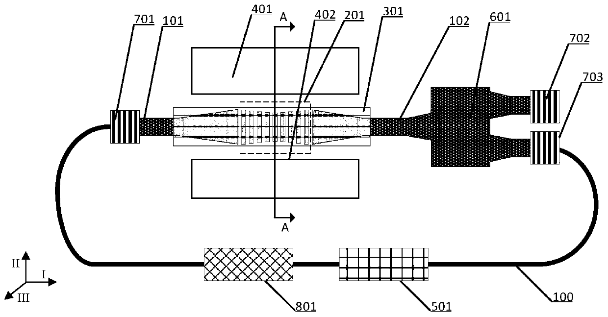
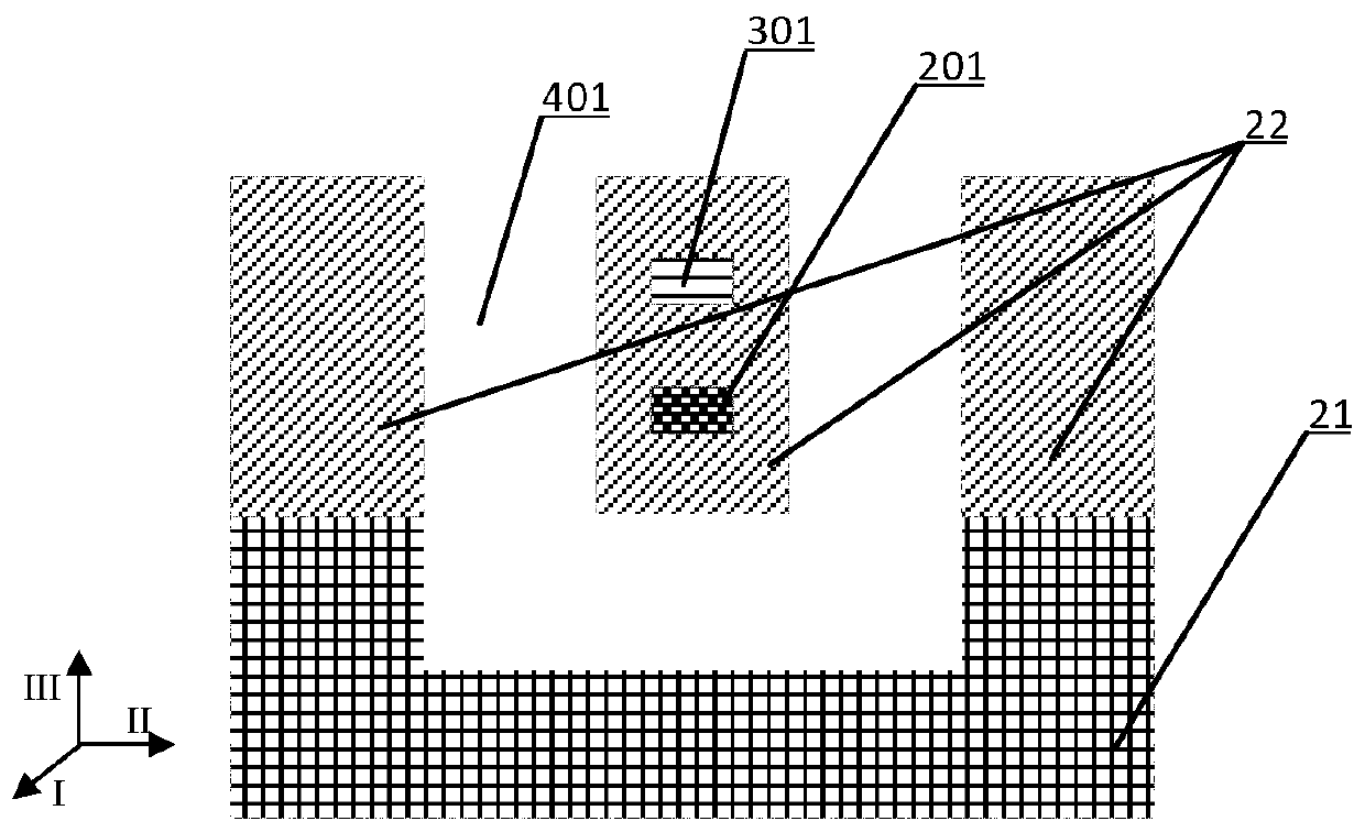
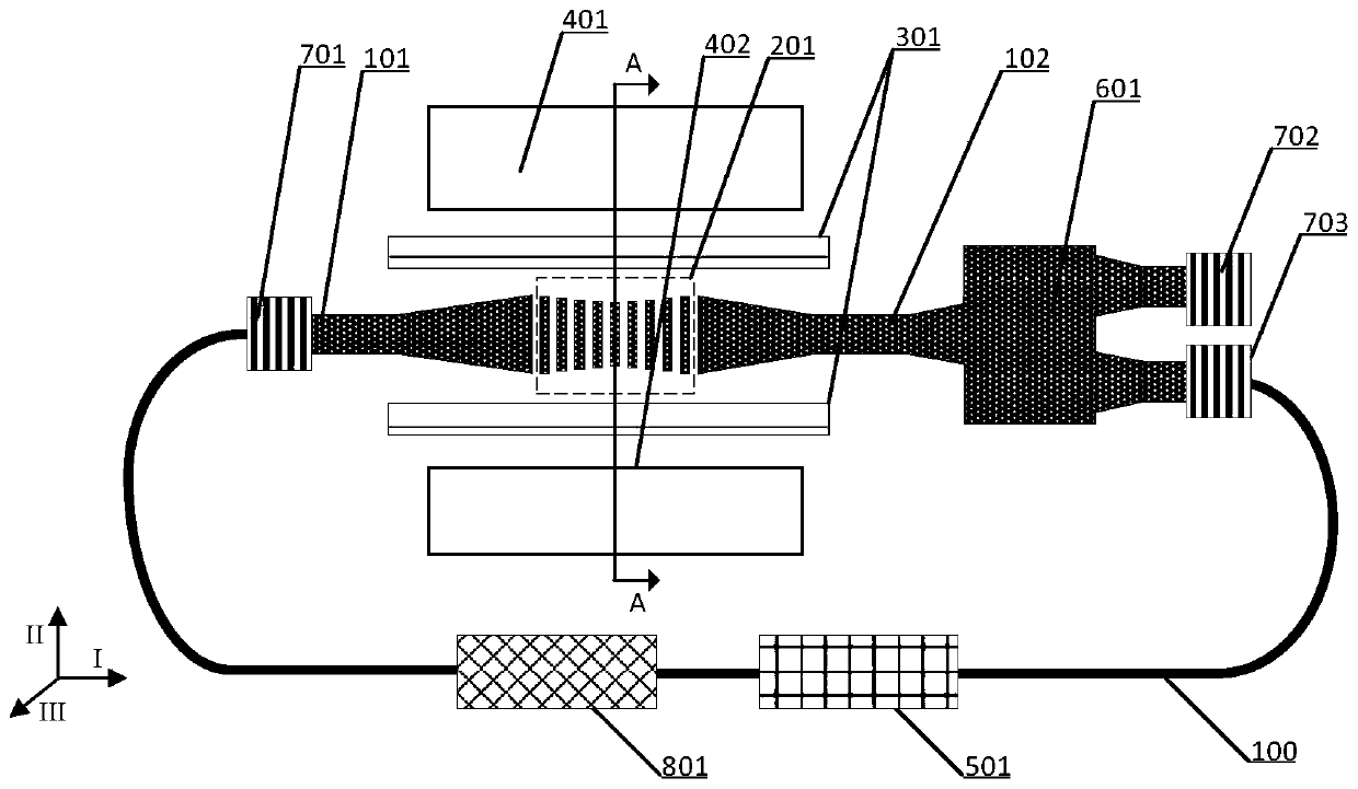
[0035] like figure 1 and figure 2 As shown, some embodiments of the present invention provide a tunable laser comprising:
[0036] Silicon substrate 21, its length, width and height directions are respectively defined as the I direction, the II direction and the III direction; and formed on the silicon substrate 21:
[0037] Optical input port 701, which is used for the input of light waves;
[0038] The first optical waveguide 101, which is used for the coupling-in of light waves from the optical input port 701;
[0039] A photonic crystal cavity 201, which is used to select and adjust the resonance wavelength of the optical wave coupled in throu...
PUM
 Abstract
Description
Claims
Application Information