Laser manufacturing method and laser

A manufacturing method and laser technology, applied in the field of communication, can solve problems such as crystal defects, lower reliability of lasers, easy mode hopping, etc.

Pending Publication Date: 2022-05-17
ZHONGXING PHOTONICS TECH CO LTD
View PDF0 Cites 0 Cited by
  • Summary
  • Abstract
  • Description
  • Claims
  • Application Information

AI Technical Summary

Problems solved by technology

Among them, the tunable DFB laser with compact structure can change the lasing wavelength by injecting current in the phase region, but the DFB integrated laser with this structure, the middle phase region is the butt-grown bulk material (not including the grating), and the DFB on both sides The initial phase of t

Method used


Image

  • Laser manufacturing method and laser
  • Laser manufacturing method and laser
  • Laser manufacturing method and laser

Examples


Embodiment 1

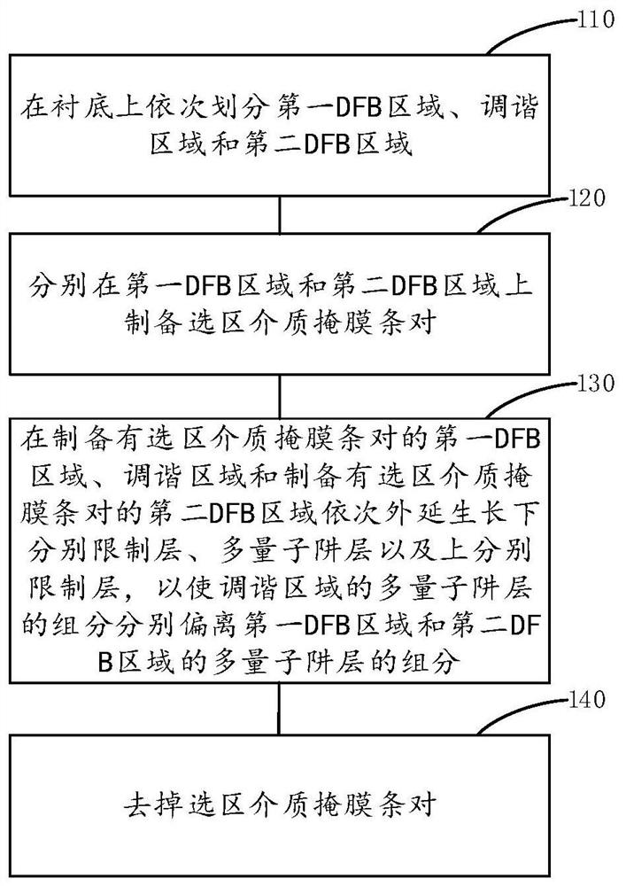
[0115] Embodiment one, such as Figure 7 as shown, Figure 7 It is a top view of the laser. In one embodiment, the laser can be divided into three areas (including the first DFB area A1, the second DFB area A2 and the tuning area T1), and the first DFB area A1 and the second DFB area can be A2 is separately arranged on both sides of the laser, and the tuning region T1 is arranged in the middle of the first DFB region A1 and the second DFB region A2; it can be separately prepared in the first DFB region A1 and the second DFB region A2 on the substrate 910 The pair of selected area dielectric mask strips, the selected area pair of dielectric mask strips includes a first selected area pair of dielectric mask strips and a second selected area pair of dielectric mask strips, wherein the first selected area pair of dielectric mask strips is prepared with a second A dielectric mask strip 710 and a second dielectric mask strip 720, the second DFB region is prepared with a pair of sec...

Embodiment 2

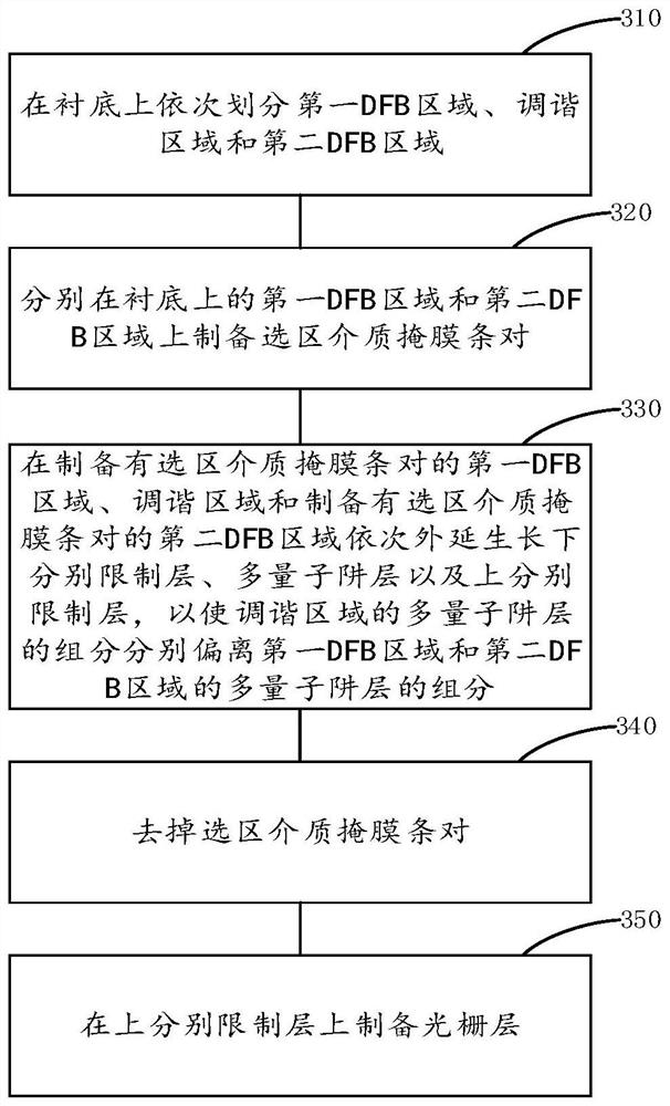
[0123] Embodiment two, such as Figure 14 As shown, the pair of selective area dielectric mask strips 1410 can also be fabricated in the middle of the tuning area, as Figure 10 As shown, during epitaxial growth at this time, the number, thickness and composition parameters of the wells in the multi-quantum well layer 940 are in accordance with the DFB laser material structure in the non-large area region (the first DFB region A1 and the second DFB region A2). Due to the increased thickness of the dielectric mask strips and the combined effect of rich indium, the material composition of the tuning region in the multi-quantum well layer 940 and the first DFB region A1 and the second DFB region A2 in the multi-quantum well layer 940 The material components in the DFB are different, the wavelength of the spontaneous emission in the tuning region is greater than the wavelength in the DFB region, and when the Bragg lasing wavelength is designed to be at the peak-peak value of the a...

Embodiment 3

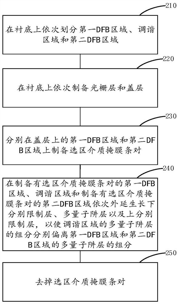
[0124] Embodiment three, such as Figure 15As shown, the pair of selective dielectric mask strips can be prepared in the first DFB area A1 and the second DFB area A2, and the grating is prepared as an N-face grating 1510, and the N-face grating 1510 can be prepared under the active layer, then the fabrication of the laser The method may include the following steps: the laser may be divided into three areas (including the first DFB area A1, the second DFB area A2 and the tuning area T1), and the first DFB area A1 and the second DFB area A2 may be separately arranged on the laser Set the tuning region T1 in the middle of the first DFB region A1 and the second DFB region A2, grow a grating layer and an InP capping layer on the substrate 910, and then prepare a specific periodic N-face grating 1510, and then Prepare a pair of selective dielectric mask strips on the first DFB region A1 and the second DFB region A2 of the epitaxial wafer for preparing the N-face grating 1510, and th...


PUM


Abstract

The embodiment of the invention discloses a manufacturing method of a laser and the laser. The manufacturing method comprises the following steps: sequentially dividing a first distributed feedback (DFB) region, a tuning region and a second DFB region on a substrate; respectively preparing selected area dielectric mask strip pairs on the first DFB region and the second DFB region, or preparing selected area dielectric mask strip pairs on the tuning region; sequentially epitaxially growing a lower respective limiting layer, a multi-quantum well layer and an upper respective limiting layer in a first DFB region and a tuning region which are provided with selected region dielectric mask strip pairs, and a second DFB region which is provided with selected region dielectric mask strip pairs, or in the first DFB region, the tuning region and the second DFB region which are provided with selected region dielectric mask strip pairs; the components of the multi-quantum well layer in the tuning region are respectively deviated from the components of the multi-quantum well layer in the first DFB region and the second DFB region; removing the selected area medium mask strip pairs; the laser manufactured through the manufacturing method is high in reliability, and the wavelength tuning range of the laser can be enlarged.

Description

technical field [0001] Embodiments of the present invention relate to but are not limited to the communication field, and in particular, relate to a method for manufacturing a laser and the laser. Background technique [0002] In recent years, with the rapid increase in the amount of information transmission in the field of optical communication, wavelength division multiplexing (WDM) systems that can effectively expand communication capacity have developed rapidly, and wavelength-tunable semiconductor lasers that can be used to build more effective communication systems have attracted widespread attention. Semiconductor lasers with good stability, large wavelength tuning range, compact structure, low power consumption and high-speed operation are of great significance in the field of optical communication. [0003] At present, tunable semiconductor lasers mainly include DBR (Distributed Bragg Reflection, distributed Bragg reflector) laser and DFB (Distributed Feedback, dist...

Claims


Application Information

Patent Timeline
IPC IPC(8): H01S5/12H01S5/32H01S5/34
CPCH01S5/12H01S5/3216H01S5/34H01S2304/00H01S5/2077H01S5/1243H01S5/1246H01S5/06258H01S5/2272
Inventor 邓秋芳
Owner ZHONGXING PHOTONICS TECH CO LTD
Why Eureka
Try Eureka