Fabrication process of multi-layer semiconductor printed circuit board

A technology of printed circuit board and preparation process, applied in the direction of multi-layer circuit manufacturing, printed circuit components, etc., can solve the problem that single and double-sided boards cannot meet the requirements of design and use, and achieve the improvement of signal transmission speed and connection. Shortening, small size effect

Inactive Publication Date: 2019-05-17
博罗县亿阳电子有限公司
View PDF4 Cites 5 Cited by
  • Summary
  • Abstract
  • Description
  • Claims
  • Application Information

AI Technical Summary

Problems solved by technology

[0002] Printed circuit board refers to the assembly board that selectively processes mounting holes, connecting wires and assembling and welding electronic components on the insulating substrate to realize the electrical connection between components. Due to the rapid development of high technology, large Some electronic products are developing in the direction of multi-layering. The traditional single-sided and double-sided panels can no longer meet the requirements of design and use. In order to meet the requirements of the market, therefore, designing a preparation process for multi-layer semiconductor printed circuit boards is very necessary

Method used


Image

  • Fabrication process of multi-layer semiconductor printed circuit board

Examples


Embodiment Construction

[0023] The following will clearly and completely describe the technical solutions in the embodiments of the present invention with reference to the accompanying drawings in the embodiments of the present invention. Obviously, the described embodiments are only some, not all, embodiments of the present invention. Based on the embodiments of the present invention, all other embodiments obtained by persons of ordinary skill in the art without making creative efforts belong to the protection scope of the present invention.

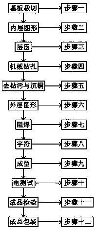
[0024] see figure 1 , the present invention provides a technical solution:

[0025] A preparation process for a multilayer semiconductor printed circuit board, comprising the following steps: Step 1, substrate cutting; Step 2, inner layer graphics; Step 3, lamination; Step 4, mechanical drilling; Step 5, desmearing Step 6, outer layer graphics; Step 7, solder mask; Step 8, characters; Step 9, molding; Step 10, electrical test; Step 11, finished product inspec...


PUM


Abstract

The invention discloses a fabrication process of a multi-layer semiconductor printed circuit board. The fabrication process comprises the following steps of 1, substrate cutting; 2, inner-layer pattern; 3, lamination; 4, mechanical drilling; 5, drill dirt removal and copper deposition, 6, outer-layer pattern; 7, resistant soldering; 8, character making; 9, formation; 10, electrical test; 11, finished product inspection; and 12, finished product package. In the step 1, an original copper-coated plate is cut to form a plate which can be fabricated on a production line. According to the fabrication process of the multi-layer semiconductor printed circuit board, the multi-layer printed circuit board is fabricated by the step process; compared with a single- and dual-layer circuit board, the multi-layer semiconductor printed circuit board has the advantages of high assembly density, small size and good shielding effect, a connection line between electrical component is shortened, the signaltransmission speed is improved, and wiring is facilitated; and for a high-frequency circuit, a ground line is added, so that constant low impedance of a signal line on ground is formed.

Description

technical field [0001] The invention relates to the technical field of printed circuit board preparation, in particular to a preparation process of a multilayer semiconductor printed circuit board. Background technique [0002] Printed circuit board refers to the assembly board that selectively processes mounting holes, connecting wires and assembling and welding electronic components on the insulating substrate to realize the electrical connection between components. Due to the rapid development of high technology, large Some electronic products are developing in the direction of multi-layering. The traditional single-sided and double-sided panels can no longer meet the requirements of design and use. In order to meet the requirements of the market, therefore, designing a preparation process for multi-layer semiconductor printed circuit boards is very necessary. Contents of the invention [0003] The object of the present invention is to provide a process for preparing a...

Claims


Application Information

Patent Timeline
Patent Type & Authority Applications(China)
IPC IPC(8): H05K1/02H05K3/46
Inventor 杨勇张波涛
Owner 博罗县亿阳电子有限公司
Why Eureka
Try Eureka