Encapsulation structure and electronic device

A packaging structure and sub-slot technology, applied to circuits, electrical components, electrical solid devices, etc., can solve the problems of increasing the risk of board-level solder ball breakage, displacement of bare chips and heat dissipation covers, and excessive operating temperature of bare chips. Achieve the effects of reducing the risk of delamination, enhancing board-level reliability, and reducing peeling stress

Inactive Publication Date: 2019-05-21
HUAWEI TECH CO LTD
View PDF7 Cites 6 Cited by
  • Summary
  • Abstract
  • Description
  • Claims
  • Application Information

AI Technical Summary

Problems solved by technology

However, due to the thermal expansion (CTE) mismatch between the various packaging materials, the thermal stress during the operation of the die will cause the package to warp and deform, resulting in relative displacement between the die and the heat sink cover, which in turn will cause delamination of the thermal conductive adhesive
The delamination of the thermal conductive adhesive will interrupt the heat dissipation channel, and the heat cannot be diffused from the die, resulting in excessive operating temperature of the die, deterioration of the electrical performance of the die, accelerated die aging, and even damage to the die
Secondly, although the high rigidity of the heat dissipation cover limits the warping deformation of the package, it also increases the risk of board-level solder ball fracture

Method used


Image

  • Encapsulation structure and electronic device
  • Encapsulation structure and electronic device
  • Encapsulation structure and electronic device

Examples


Embodiment Construction

[0037] Embodiments of the present invention will be described below with reference to the drawings in the embodiments of the present invention.

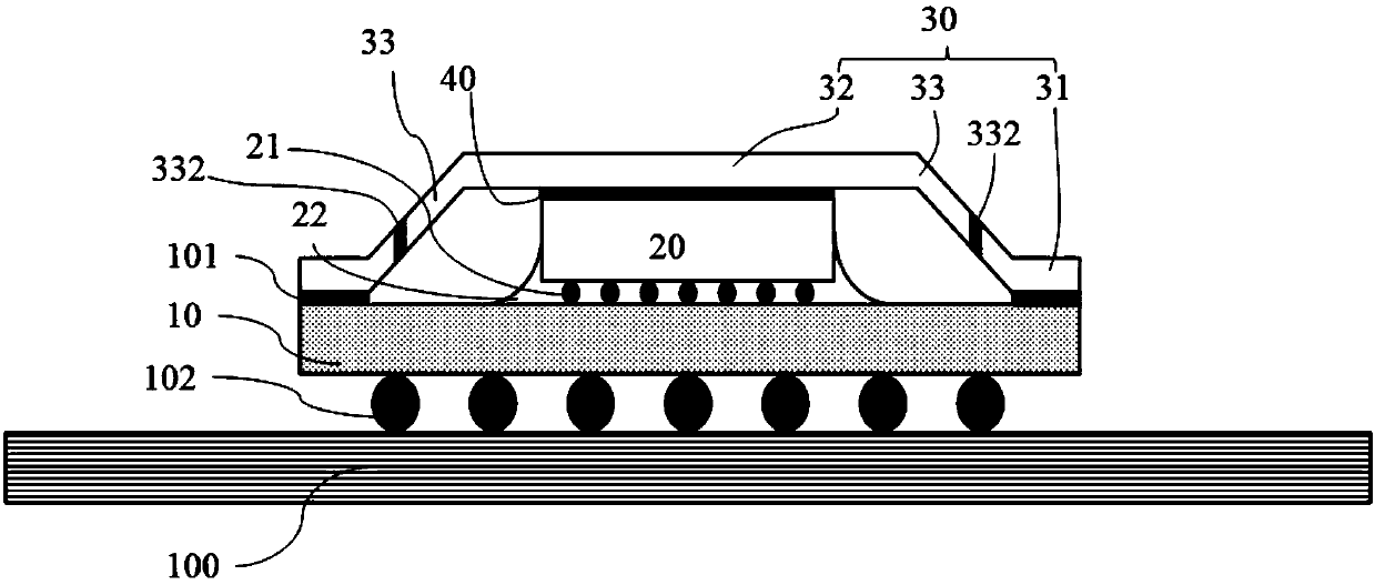
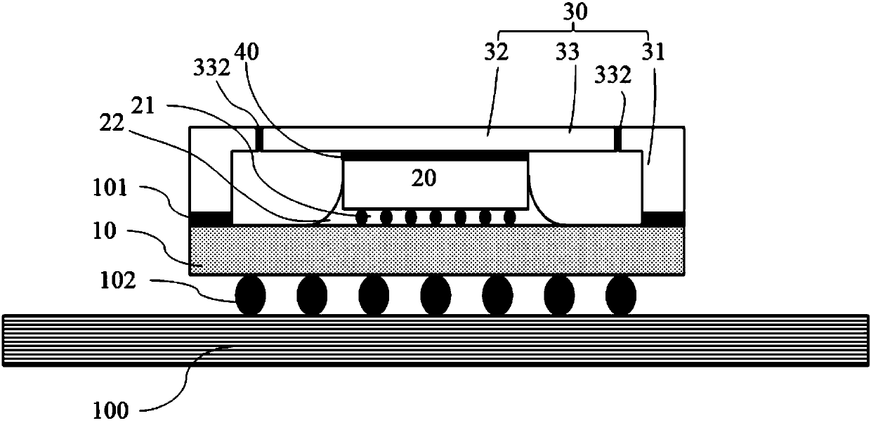
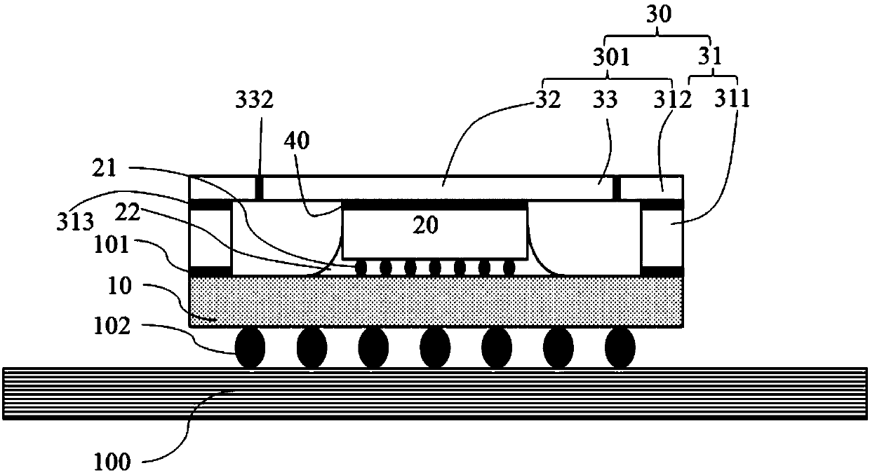
[0038] An embodiment of the present invention provides a packaging structure, which is applied to an electronic device and fixed on a circuit board in the circuit device. In one embodiment, the encapsulation structure can be applied to electronic components with high heat generation.

[0039] figure 1 The package structure shown includes a substrate 10, a die 20, and a heat dissipation cover 30, the die 20 is mounted on the surface of the substrate 10, the heat dissipation cover 30 is connected to the substrate 10 and covers the die the periphery of the sheet 20. The substrate 10 can be a metal substrate, a ceramic substrate or a PCB board. The upper surface of the substrate 10 is mounted with bare chips 20 and other electronic components, and the lower surface of the substrate 10 is used for electrical connection with the circuit ...


PUM


Abstract

An embodiment of the invention discloses an encapsulation structure comprising a substrate, a bare chip and a heat dissipation cover, wherein the bare chip is mounted on the surface of the substrate,the heat dissipation cover is connected to the substrate and covers the periphery of the bare chip, the heat dissipation cover comprises a fixing portion and a heat conduction portion, the fixing portion is fixedly connected to the substrate, the heat conduction portion directly faces the surface, facing away from the substrate, of the bare chip, a heat conduction adhesive is provided between thebare chip and the heat conduction portion, and a slot is provided between the heat conduction portion and the fixing portion to reduce the rigidity of the heat dissipation cover. The embodiment of theinvention further discloses an electronic device. The encapsulation structure and electronic device can reduce the risk of the heat conduction adhesive being delaminated and increase the reliabilityof the encapsulation structure.

Description

technical field [0001] The invention relates to packaging technology, in particular to an electronic device using a packaging structure including a heat dissipation cover. Background technique [0002] With the improvement of chip integration channel rate, system application requires further improvement of integration level, and the number of chip high-speed signal channels has increased significantly, resulting in continuous increase of chip power consumption; in order to ensure the realization of link drive capability, signal isolation and system interconnection, packaging The size is also gradually increased. However, the ensuing package heat problem and stress problem are more severe than small-size low-power chip packages; in addition, the gradual popularization of 2.5D / 3D packages also puts forward higher requirements for package size and package heat dissipation. At present, the common packaging form adopts the structure that the back of the die is connected to the h...

Claims


Application Information

Patent Timeline
Patent Type & Authority Applications(China)
IPC IPC(8): H01L23/00H01L23/367
CPCH01L2224/73204H01L2224/73253H01L2924/15311H01L2924/16195H01L23/00H01L23/10H01L23/34H01L23/367
Inventor 符会利蔺贤哲戈云飞张弛郭健炜
Owner HUAWEI TECH CO LTD
Why Eureka
Try Eureka