Transistor with high electron mobility and manufacturing method thereof

A technology of high electron mobility and manufacturing method, which is applied in the field of high electron mobility transistors and its manufacturing, and can solve the problems of low device reliability, low breakdown voltage, and low gate input impedance

Pending Publication Date: 2019-05-21
珠海镓未来科技有限公司
View PDF2 Cites 4 Cited by
  • Summary
  • Abstract
  • Description
  • Claims
  • Application Information

AI Technical Summary

Problems solved by technology

Therefore, there are disadvantages such as low gate turn-on voltage, small gate input voltage swing, susceptible to external signal interference, large gate leakage, low gate withstand voltage and low breakdown voltage, and low gate input impedance, which lead to the reliability of the device. Low sex
However, due to the existence of problems such as interface states and bulk charges, if an insulating dielectric layer is added to the gate, the performance of the device will be significantly reduced

Method used


Image

  • Transistor with high electron mobility and manufacturing method thereof
  • Transistor with high electron mobility and manufacturing method thereof
  • Transistor with high electron mobility and manufacturing method thereof

Examples


Embodiment Construction

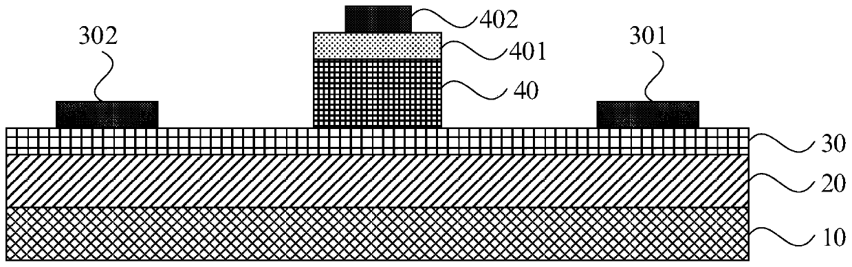
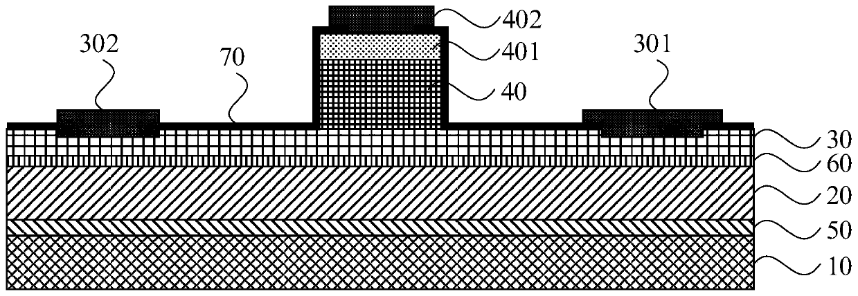
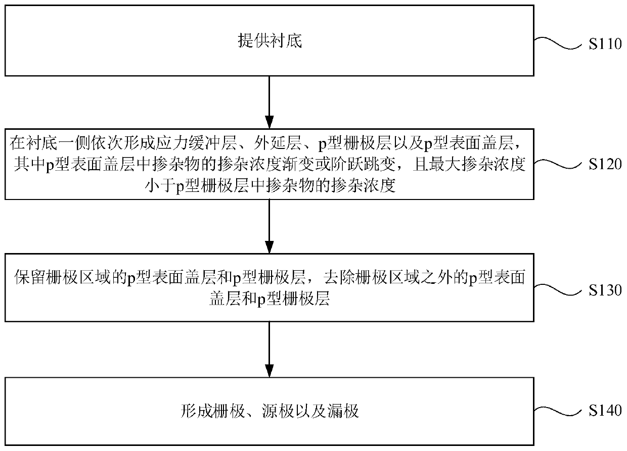
[0039] The present invention will be further described in detail below with reference to the drawings and embodiments. It can be understood that the specific embodiments described here are only used to explain the present invention, but not to limit the present invention. In addition, it should be noted that, for ease of description, the drawings only show a part but not all of the structure related to the present invention. In addition, the present invention provides examples of various specific processes and materials, but as those skilled in the art can understand, the present invention may not be implemented according to these specific details. Unless otherwise specified in the following, all parts of the device can be implemented using processes and materials known in the art. In addition, the structure in which the first feature is "on" the second feature described below may include an embodiment in which the first and second features are formed in direct contact, or may...


PUM


Abstract

The embodiment of the invention discloses a transistor with high electron mobility and a manufacturing method thereof. The transistor with the high electron mobility comprises a substrate; a stress buffer layer and an epitaxial layer sequentially arranged on one side of the substrate; a source, a drain and a p-type grid layer arranged on one side, far away from the substrate, of the epitaxial layer; and a p-type surface cover layer and a grid sequentially stacked on one side, far away from the substrate, of the p-type grid layer; wherein the doping density of a dopant in the p-type surface cover layer is gradually changed or jumped, and the maximum doping density is less than the doping density of the dopant in the p-type grid layer. According to the technical scheme provided by the embodiment of the invention, the grid threshold voltage, the grid breakdown voltage, the grid input voltage swing and the grid input impedance of the device are effectively improved, and the stability and reliability of the device are improved.

Description

Technical field [0001] The embodiment of the present invention relates to semiconductor device technology, in particular to a high electron mobility transistor and a manufacturing method thereof. Background technique [0002] The third-generation semiconductor materials represented by gallium nitride (GaN) have the characteristics of forbidden bandwidth, high critical breakdown electric field, good thermal conductivity, high melting point, high saturation mobility of electrons, and radiation resistance. They are suitable for the production of high voltage and high power , High-performance electronic devices such as high frequency, high temperature resistance and radiation resistance. Its applications include power electronic devices, radio frequency devices, optoelectronic devices and other fields, and are core electronic components for applications such as solid-state lighting, storage, communications, consumer electronics, and new energy vehicles and smart grids. At present, t...

Claims


Application Information

Patent Timeline
Patent Type & Authority Applications(China)
IPC IPC(8): H01L29/06H01L29/778H01L21/335
Inventor 于洪宇曾凡明
Owner 珠海镓未来科技有限公司
Why Eureka
Try Eureka