Epitaxial wafer of light-emitting diode and preparation method thereof

A technology for light-emitting diodes and epitaxial wafers, which is applied in the fields of nanotechnology, electrical components, and nanotechnology for materials and surface science, and can solve the problems of poor crystal quality of light-emitting diodes, affecting the quality of GaN layers, and large grain boundary defects. , to achieve the effect of improving crystal quality, small difference in growth volume, and improving crystal quality

Active Publication Date: 2019-05-21
HC SEMITEK ZHEJIANG CO LTD
View PDF2 Cites 6 Cited by
  • Summary
  • Abstract
  • Description
  • Claims
  • Application Information

AI Technical Summary

Problems solved by technology

After Ga atoms and N atoms are concentrated at the nucleation point to form an island structure in the GaN nucleation layer, Ga atoms and N atoms are likely to continue to concentrate on the island structure to form an oversized cluster, and due to the If the distance between them is large, the atoms in each cluster will also appear to move, diffuse and merge during the subsequent growth process of the undoped GaN layer. On the one hand, more lattice distortions and defects will appear during the process of moving and diffusing. , on the other hand, the unevenness of the volume of each cluster also makes the grain boundary defects at the merger between the clusters larger, and it is easier to form high-angle grain boundaries, which will affect the quality of the final undoped GaN layer. Resulting in poorer overall crystal quality of the resulting LED

Method used


Image

  • Epitaxial wafer of light-emitting diode and preparation method thereof
  • Epitaxial wafer of light-emitting diode and preparation method thereof
  • Epitaxial wafer of light-emitting diode and preparation method thereof

Examples


Embodiment Construction

[0030] In order to make the object, technical solution and advantages of the present invention clearer, the implementation manner of the present invention will be further described in detail below in conjunction with the accompanying drawings.

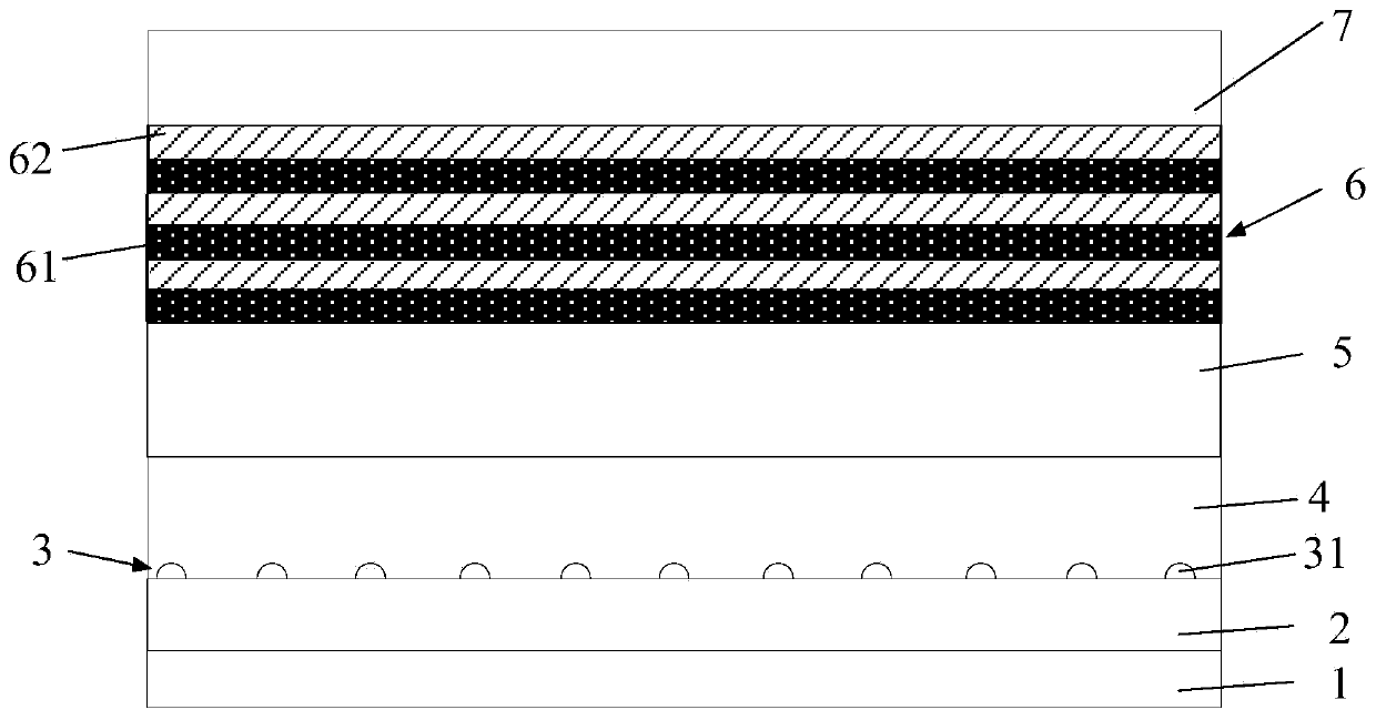
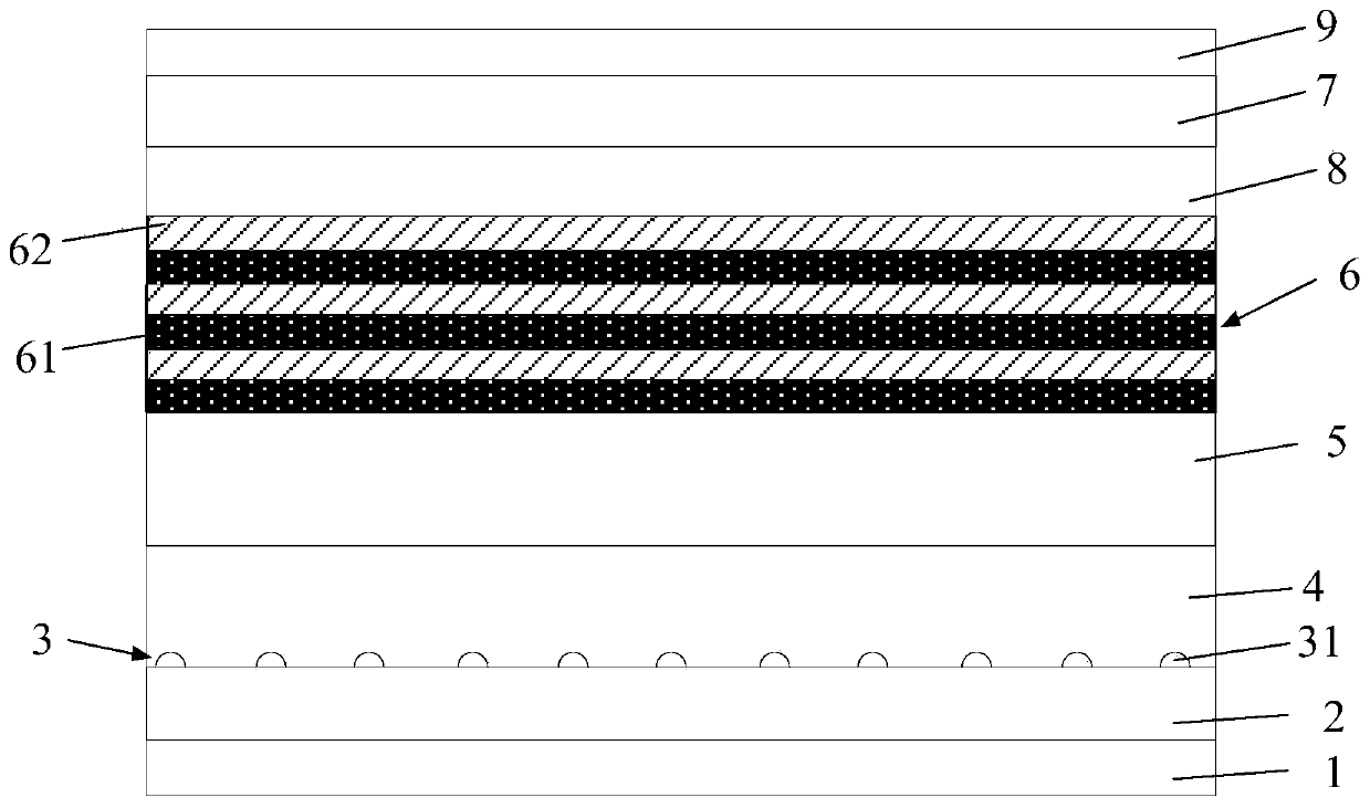
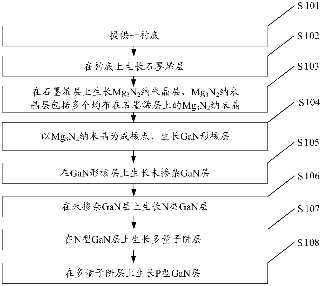
[0031] figure 1 It is a schematic structural diagram of an epitaxial wafer of a light emitting diode provided by an embodiment of the present invention, as shown in figure 1 As shown, the epitaxial wafer includes a substrate 1 and a graphene layer 2, Mg 3 N 2 Nanocrystalline layer 3, GaN nucleation layer (not shown in the figure), undoped GaN layer 4, N-type GaN layer 5, multiple quantum well layer 6 and P-type GaN layer 7, wherein Mg 3 N 2 The nanocrystalline layer 3 includes a plurality of Mg evenly distributed on the graphene layer 2 3 N 2 Nanocrystalline 31, Mg 3 N 2 The nanocrystal 31 is the nucleation point of the GaN nucleation layer, and the GaN nucleation layer is doped with Mg.

[0032] Laminate Mg on graphene layer 2...


PUM

PropertyMeasurementUnit
thicknessaaaaaaaaaa
thicknessaaaaaaaaaa
thicknessaaaaaaaaaa

Abstract

The invention discloses an epitaxial wafer of a light-emitting diode and a preparation method thereof and belongs to the field of light-emitting diode manufacturing. The epitaxial wafer has the beneficial effects that a Mg3N2 nanocrystalline layer is laminated on a graphene layer, a plurality of Mg3N2 nanocrystals in the Mg3N2 nanocrystalline layer have low surface potential energy points and highchemical activity and can serve as nucleation points of a GaN nucleating layer and the GaN nucleating layer is easier to grow on the Mg3N2 nanocrystals to ensure that a plurality of island structurescan be uniformly formed on the graphene layer by the GaN nucleation layer; when an un-doped GaN layer continues to grow, more Ga atoms and N atoms are attracted by the island structures to continue to grow; and the distance between the island structures is appropriate and the migration and the diffusion of the atoms are relatively less, thereby reducing the lattice distortion and defects caused by atoms on the island structures in the moving diffusion process and increasing the crystal quality of the un-doped GaN layer.

Description

technical field [0001] The invention relates to the field of light-emitting diode manufacturing, in particular to an epitaxial wafer of a light-emitting diode and a preparation method thereof. Background technique [0002] Light-emitting diodes are semiconductor diodes that can convert electrical energy into light energy. They have the advantages of small size, long life, and low power consumption. They are currently widely used in automotive signal lights, traffic lights, display screens, and lighting equipment. The epitaxial wafer is the basic structure for making light-emitting diodes. The structure of the epitaxial wafer includes a substrate and a graphene layer grown on the substrate in sequence, a GaN nucleation layer, an undoped GaN layer, an N-type GaN layer, and a multi-quantum well layer. And the P-type GaN layer, wherein the GaN nucleation layer includes a plurality of island structures distributed on the graphene layer. When the undoped GaN layer is grown, the is...

Claims


Application Information

Patent Timeline
Patent Type & Authority Applications(China)
IPC IPC(8): H01L33/02H01L33/32H01L33/00B82Y30/00
Inventor 丁涛周飚胡加辉李鹏
Owner HC SEMITEK ZHEJIANG CO LTD
Why Eureka
Try Eureka