Novel processing method of printed circuit board

A technology for printed circuit boards and processing methods, which is applied to printed circuits connected to non-printed electrical components, printed circuit components, printed circuits assembled with electrical components, etc., and can solve solder joint drop-off, soldering failure, and poor heat dissipation and other problems, to achieve the effect of preventing sharp corner scratches, preventing collision damage, and ensuring performance

Active Publication Date: 2019-05-21
深圳市满坤电子有限公司
View PDF3 Cites 3 Cited by
  • Summary
  • Abstract
  • Description
  • Claims
  • Application Information

AI Technical Summary

Problems solved by technology

Although these substrates have excellent electrical properties and processing properties, they have poor heat dissipation. As a heat dissipation path for high-heating components, it is almost impossible to expect the heat to be conducted by the resin of the PCB itself, but to dissipate heat from the surface of the component to the surrounding air. Electronic products have entered the era of component miniaturization, high-density installation, and high-heating assembly. It is not enough to rely on the surface of components with a very small surface area to dissipate heat. At the same time, due to the extensive use of surface-mounted components such as QFP and BGA, components A large amount of heat generated is transmitted to the PCB board. Therefore, the best way to solve the heat dissipation is to improve the heat dissipation capacity of the PCB itself that is in direct contact with the heating element, and conduct or dissipate it through the PCB board.
[0004] The second is the welding problem. During the welding process of the printed circuit board, due to the deformation of the circuit board, some of the soldered parts of the printed circuit board have protrusions and some have depressions.
Thin welds will be formed at the raised solder joints, that is to say, the welding at this position is not firm, and the solder joints will fall off after a long time, and the welding will fail; The position is raised, causing the solder joints to be unable to contact with the recessed parts, thus forming an empty soldering phenomenon. Like thin soldering, the welding of the recessed parts will also cause the solder joints to fall off within a certain period of time, and the welding will fail, thus affecting the service life of electronic products.
[0005] The third is the problem of deformation. High temperature heating and insufficient thickness of the substrate can easily lead to deformation of the printed circuit board. The deformation will weaken the strength of the board, the copper foil on the board will fall off, and the soldering parts on the board will fall off, resulting in the scrapping of the circuit board.

Method used


Image

  • Novel processing method of printed circuit board
  • Novel processing method of printed circuit board
  • Novel processing method of printed circuit board

Examples


Embodiment Construction

[0030] The following will clearly and completely describe the technical solutions in the embodiments of the present invention with reference to the drawings in the embodiments of the present invention.

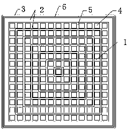
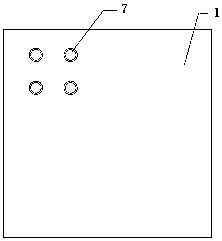
[0031] Such as Figures 1 to 4 A new processing method for printed circuit boards shown includes the following steps: Step 1, material cutting: take the raw materials and place them on the material cutting machine, and cut out the required copper-clad substrate 1 according to the size required by the production instruction sheet ;Step 2, Drilling: First use a pin machine to punch some pin holes on the short side of the copper-clad substrate, and then fix the combined board after the pin holes are punched on the workbench of the CNC drilling machine, and set the main shaft of the drilling machine Rotational speed and falling speed of the knife, drill holes on the above combination plate, after the combination plate is drilled, remove the combination plate from the workbench of ...


PUM

PropertyMeasurementUnit
Thicknessaaaaaaaaaa

Abstract

The invention discloses a novel processing method of a printed circuit board. The novel processing method comprises the following steps: cutting, drilling, hole metalizing, entire board electroplatingand copper-adding, pattern transferring, pattern electroplating, membrane stripping, etching and tin stripping, solder masking and surface treating, opening a threaded weld leg hole, CNC forming, andadding a radiating reinforced layer; a layer of carbon fiber heat-conducting silica gel sheet is adhered at each of a lateral of a circuit board and non-circuit diagram regions of the circuit board,so that the heat of the printed circuit board can be timely conducted and diffused, and the use performance of the printed circuit board under the high heating condition of the component can be well guaranteed; the carbon fiber has good mechanical strength, the heat-conducting silica gel sheets of the carbon fiber can effectively prevent the circuit board from deforming under a pressed and heatedcondition; by arranging the threaded weld leg holes on the printed circuit board, each threaded groove in the soldering hole is filled with soldering liquid, the soldering is extremely firm after thesolidification, and the welding foot cannot easily fall off.

Description

technical field [0001] The invention belongs to the technical field of printed circuit board processing, and in particular relates to a novel processing method of printed circuit boards. Background technique [0002] In recent years, the focus of the printed circuit board market has shifted from computers to communications. In the past two years, it has shifted to mobile terminals such as smart phones and tablet computers. Printed circuit boards are all developing towards high-density and thin lines. There are also many problems that need to be paid attention to in terms of processing technology. [0003] One is the problem of heat generation. At present, the widely used printed circuit board (referred to as PCB) board is copper-clad / epoxy glass cloth substrate or phenolic resin glass cloth substrate, and a small amount of paper-based copper-clad board is used. Although these substrates have excellent electrical properties and processing properties, they have poor heat diss...

Claims


Application Information

Patent Timeline
IPC IPC(8): H05K1/02H05K1/11H05K1/18H05K3/34
Inventor 洪俊城
Owner 深圳市满坤电子有限公司
Why Eureka
Try Eureka