Thin film packaged LED display array module

A display array and thin film packaging technology, applied in identification devices, instruments, etc., can solve problems such as affecting production efficiency and display effect, poor module ink color consistency, crosstalk of light-emitting pixels, etc., to achieve good color consistency, simple production process, The effect of a large viewing angle

Inactive Publication Date: 2019-05-28
CHANGCHUN CEDAR ELECTRONICS TECH CO LTD
View PDF10 Cites 7 Cited by
  • Summary
  • Abstract
  • Description
  • Claims
  • Application Information

AI Technical Summary

Problems solved by technology

After the LED chip is connected to the display substrate, it is packaged by dispensing, potting, and molding. However, these packaging processes still have problems such as complex process, poor ink color consistency of the module, and crosstalk between luminous pixels, which affect production efficiency and display effect.

Method used


Image

  • Thin film packaged LED display array module
  • Thin film packaged LED display array module
  • Thin film packaged LED display array module

Examples


Embodiment 1

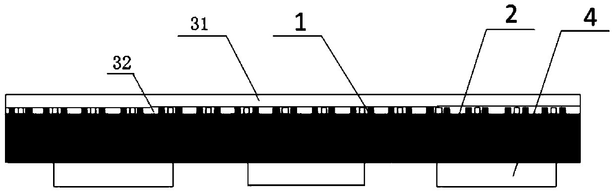
[0025] An LED display array module arranged in a dot matrix with a dot pitch of d=1.25mm and a resolution of 64×64.

[0026] Such as figure 1 , 2 As shown, the film-encapsulated LED display array module of the present invention is formed by splicing a plurality of LED display modules, and the LED display module includes a driver IC4, a display substrate 2, an LED wafer 1 and a layer of film 31, and the film 31 The thickness is 0.1-0.8mm. The driver IC 4 is welded on the rear surface of the display substrate 2 , the LED chip 1 is fixed on the front surface of the display substrate 2 , and the film 31 is pasted on the front surface of the display substrate. The film 31 is made of epoxy resin; the LED wafer 1 is an ordinary red, green and blue LED light-emitting chip; the display substrate 2 is a printed circuit board PCB.

[0027] The film 31 is encapsulated on the front surface of the display substrate 2 by the following method: first, a layer of buffer glue 32 is sprayed on...

Embodiment 2

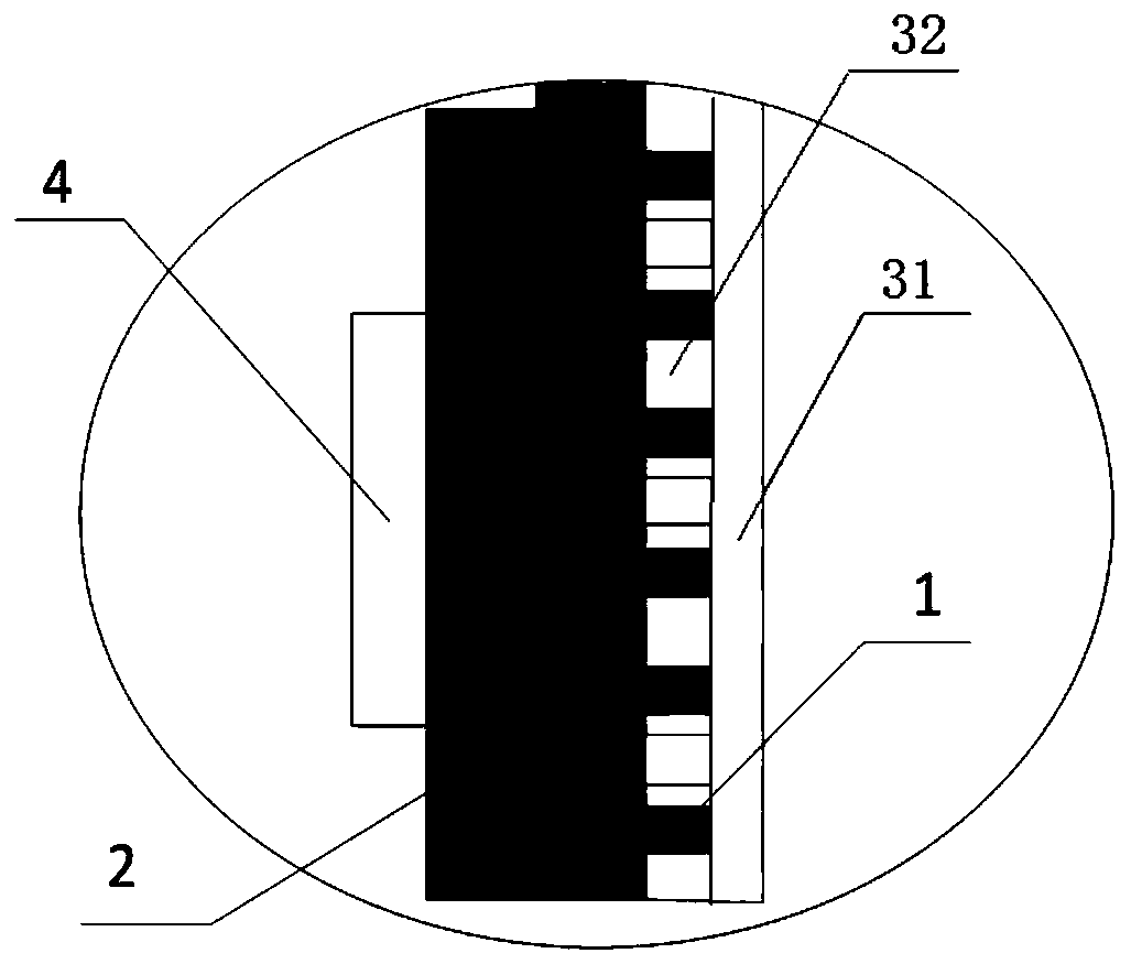
[0031] An LED display array module with a dot pitch of d=1.25mm and a dot matrix with a resolution of 64×64.

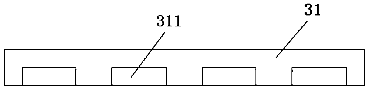
[0032] Such as image 3 , 4 , 5, the film-encapsulated LED display array module of the present invention is spliced ​​by a plurality of LED display modules, and the LED display module includes a driver IC4, a display substrate 2, an LED wafer 1 and a layer of film 31, and the film 31 has a thickness of 0.1-0.8mm; the back of the film 31 has a hole 311 corresponding to the position of the LED chip; the driver IC 4 is welded on the rear surface of the display substrate 2, the LED chip 1 is fixed on the front surface of the display substrate 2, and the film 31 is packaged on the front surface of the display substrate 2 . The film 31 is made of epoxy resin; the LED wafer 1 is an ordinary red, green and blue LED light-emitting chip; the display substrate 2 is a printed circuit board PCB.

[0033] The film 31 is encapsulated on the front surface of the display substrate ...

Embodiment 3

[0037] Such as Figure 6 , 7 , 8, the film-encapsulated LED display array module of the present invention is spliced ​​by a plurality of LED display modules, and the LED display module includes a driver IC4, a display substrate 2, an LED wafer 1 and two layers of films, the first The thickness of the first layer of film 33 is 0.1 mm, and the thickness of the second layer of film 34 is 0.3 mm; the first layer of film 33 is black, and has a through hole 331 corresponding to the LED wafer 1; the driver IC4 is welded behind the display substrate 2 On the surface, the LED chip 1 is fixed on the front surface of the display substrate 2 , the first film 33 is packaged on the front surface of the display substrate 2 , and the second film 34 is pasted on the front surface of the first film 33 . The materials of the two layers of film are epoxy resin; the LED chip 1 is a common red, green and blue LED light-emitting chip; the display substrate 2 is a printed circuit board PCB.

[0038...


PUM


Abstract

The invention relates to a thin film packaged LED display array module. The module is formed by splicing a plurality of LED display modules, wherein the LED display module comprises a driving IC, a display substrate and an LED wafer; the driving IC is welded to the rear surface of the display substrate; the LED wafer is fixed on the front surface of the display substrate; at least one layer of thin film is further packaged on the front surface of the display substrate; and the total thickness of the thin film is 0.1-0.8 mm. The LED display array module has the advantages of large visual angleand high color consistency, meanwhile, a traditional glue filling or die pressing packaging process is omitted, a production process is simplified, the cost is reduced, and meanwhile, a splicing gap is favorably further reduced.

Description

technical field [0001] The invention belongs to the technical field of LED display screens, and relates to a film-encapsulated LED display array module. Background technique [0002] In recent years, with the continuous improvement of people's viewing demand for display devices, high-end LED displays are developing towards high density. At present, there are two main technical routes for high-density small-pitch LED displays, namely, SMD technical route and COB technical route. For the SMD technology route, on the one hand, each pixel needs to be packaged separately by high-end equipment, and the installation is more complicated, which increases the production cost; There is not much space for circuit layout, and the requirements for display performance and mask technology are added, so the potential space for smaller pixel pitch is small and the technical difficulty is great. The COB integrated packaging technology route is to directly assemble the small-sized LED chip wi...

Claims


Application Information

Patent Timeline
Patent Type & Authority Applications(China)
IPC IPC(8): G09F9/33
Inventor 程宏斌尹景隆曹慧王瑞光
Owner CHANGCHUN CEDAR ELECTRONICS TECH CO LTD
Why Eureka
Try Eureka