
Chip packaging structure and chip packaging method

A chip packaging structure, chip technology, applied in the direction of electrical components, electric solid devices, circuits, etc., can solve the problems affecting the heat dissipation performance of the chip packaging structure, and achieve the effect of improving heat dissipation efficiency

Pending Publication Date: 2019-05-31
SOUTH UNIVERSITY OF SCIENCE AND TECHNOLOGY OF CHINA +1
View PDF0 Cites 1 Cited by
  • Summary
  • Abstract
  • Description
  • Claims
  • Application Information

AI Technical Summary

Problems solved by technology

However, there is a common problem in the above-mentioned packaging structures. There are inevitably certain interfaces between the first-level packaging of the chip, the package cover, the heat sink, the vapor chamber, and different thermal interface materials. These interfaces will cause a certain interface thermal resistance. , thus affecting the heat dissipation performance of the chip package structure

Method used


Image

  • Chip packaging structure and chip packaging method
  • Chip packaging structure and chip packaging method
  • Chip packaging structure and chip packaging method

Examples


Embodiment 1

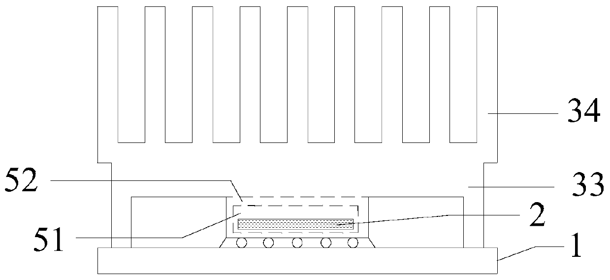
[0032] figure 2 is a schematic diagram of a chip package structure according to an embodiment of the present invention, such as figure 2 As shown, the chip package structure includes: a carrier board 1, a chip 2, a thermally conductive insulating layer and a heat sink. The heat sink includes a horizontal portion above the outer side of the thermally conductive insulating layer and a vertical portion extending from these positions close to the carrier board 1. The package cover structure 33 of the vertical part of the package cover 33 and the heat sink structure 34 formed by several groups of vertical bracket-like structures above the package cover 33, the heat conduction insulation layer includes a flexible heat conduction layer 51 wrapped on the outside of the chip 2 and a flexible heat conduction layer located on the flexible heat conduction layer. Semi-solid thermally conductive layer 52 on the outside of layer 51 . The package cover structure 33 mainly plays a certain r...

Embodiment 2

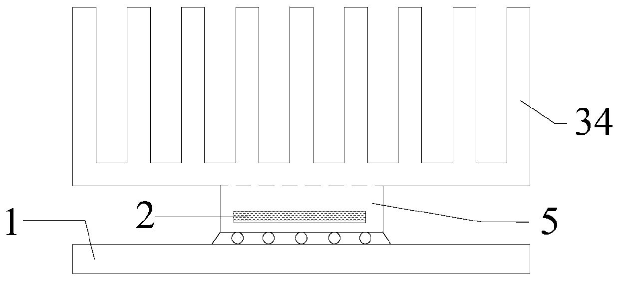
[0041] image 3 is a schematic diagram of a chip package structure according to another embodiment of the present invention. Such as figure 2As shown, the difference between the chip package structure and the embodiment 1 is that the structural setting of the package cover is omitted, and the two parts of the thermally conductive insulating layer 5 and the heat sink structure 34 are in direct contact; at the same time, in this embodiment, the flexible thermally conductive The raw materials of the layer are all silicone grease, and the raw materials of the semi-solid heat conduction layer are 60wt% of silicone grease, 20wt% of diamond, and 20wt% of silicon dioxide. Wherein, the arrangement, shape, and structure of the flexible heat-conducting layer and the semi-solid heat-conducting layer are the same as those in Embodiment 1.

Embodiment 3

[0043] Figure 4 It is a schematic diagram of a chip package structure according to another embodiment of the present invention. Such as image 3 As shown, a chip 2 is mounted on a carrier 1 , and the outer side of the chip 2 is covered with a thermally conductive insulating layer 5 . Above the thermally conductive insulating layer 5 is the package cover structure 33 , and the package cover structure 33 in this embodiment is packaged with carbon fiber-reinforced resin composite wires and boron nitride fiber-reinforced resin composite wires with high thermal conductivity. Also on the package lid structure 33 is a vapor chamber structure 35 . The amount of thermally conductive filler in the vapor chamber structure 35 is slightly more than that in the package cover structure, so as to achieve better heat dissipation.


PUM


Abstract

The invention discloses a chip packaging structure and a chip packaging method for reducing interface thermal resistance to improve the heat dissipation performance of a chip. The chip packaging structure comprises a carrier board, a chip, a thermal conductive insulating layer coating the chip and a heat dissipating component, wherein the thermal conductive insulating layer and the heat dissipating component are integrally formed. The applicant accidentally discovers during an experiment that heat dissipation members such as a traditional first-level packaging structure, a heat sink and a heatbalancing plate can be integrally formed into a whole body by 3D printing so as to eliminate the interfaces of various original parts and correspondingly eliminate the interface thermal resistance, thereby improving the heat dissipation efficiency of the chip packaging structure.

Description

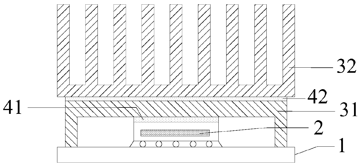
technical field [0001] The invention relates to the field of chip packaging, in particular to a chip packaging structure and a chip packaging method. Background technique [0002] Chips will generate a lot of heat during high-frequency operation, which will reduce work efficiency and shorten the service life of components. In order to ensure the normal operation of components, the heat dissipation problem must be considered during the chip packaging process. [0003] figure 1 It is a common chip packaging structure in the prior art. Such as figure 1 As shown, the package cover 31 is bonded to the bare core 2 coated with epoxy resin mounted on the carrier board 1 through the pad 6 through the thermal interface material 1 41 (TIM1). Above the package cover 31 , a heat sink 32 made of metal or metal alloy is also connected through a thermal interface material 2 42 (TIM2). Some other possible packaging structures include a vapor chamber bonded to the TIM2, or the chip is dir...

Claims


Application Information

Patent Timeline
Patent Type & Authority Applications(China)
IPC IPC(8): H01L23/29H01L23/373H01L21/56
CPCH01L2224/16225H01L2224/73204H01L2224/32225H01L2224/73253H01L2924/00
Inventor 祝渊康飞宇宋厚甫
Owner SOUTH UNIVERSITY OF SCIENCE AND TECHNOLOGY OF CHINA
Learn More