Broadband wave-absorbing metamaterial

A technology of metamaterials and structural materials, applied in the field of electronic functional structural materials, can solve problems such as large thickness and complex structure, and achieve the effect of simple structure and small volume

Inactive Publication Date: 2019-05-31
刘世丞
View PDF0 Cites 9 Cited by
  • Summary
  • Abstract
  • Description
  • Claims
  • Application Information

AI Technical Summary

Problems solved by technology

[0005] The microwave-absorbing metamaterials reported in the existing literature still cannot meet the requirements of thin thickness, light weight and

Method used


Image

  • Broadband wave-absorbing metamaterial
  • Broadband wave-absorbing metamaterial
  • Broadband wave-absorbing metamaterial

Examples


Embodiment approach 1

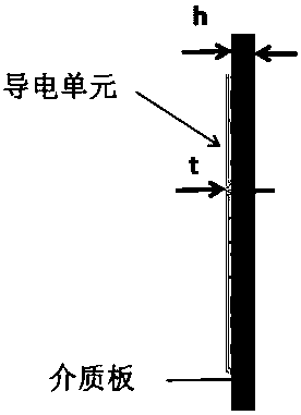
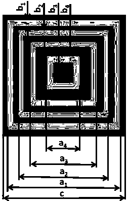
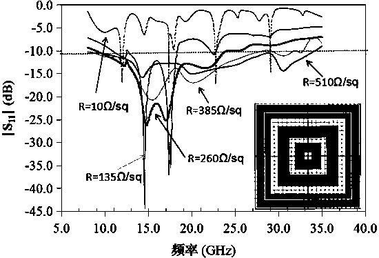
[0023] Using CST STUDIO SUITE software to carry out theoretical calculation on the model, in the structural parameters of the conductive unit (units are mm) , , , , , , , , , , the structural parameters of the dielectric plate , the material parameter of the conductive element value (in units of ) is 135, 260, 385 and 510, such as image 3 As shown, the calculation results show that this material can achieve reflection coefficient in a wide band (i.e. greater than absorption rate). Among them, in When the material is Reflection coefficients are achieved across the frequency range (i.e. greater than absorption rate). image 3 shown in The calculation results only achieve absorption peaks at specific frequency points, but fail to achieve broadband absorption.

Embodiment approach 2

[0025] Using CST STUDIO SUITE 2015 software for theoretical calculation of the model, the structural parameters of the conductive unit (units are mm) , , , , , , , , , , the structural parameter of the dielectric plate h=1mm, the value of the material parameter R of the conductive unit (the unit is ) is 260, 385 and 400, such as Figure 4 As shown, the calculation results show that this material can achieve reflection coefficient in a wide band (ie greater than 90% absorption). Among them, in and When the material achieves reflection coefficient in the frequency range of 16-60GHz .

Embodiment approach 3

[0027] Using the parameter scanning function of CST STUDIO SUITE 2015 software, set the dielectric plate as a low-loss dielectric material, the real part of its dielectric constant is in the range of 3.3 to 4.9, and the concentric square ring metamaterial structure size (in mm) is as follows Scan calculations within the range, , , , , , , , , , In the frequency range of 16-60GHz, the absorption rate of more than 90% with a bandwidth of more than 40GHz has been realized.


PUM

PropertyMeasurementUnit
Thicknessaaaaaaaaaa

Abstract

Disclosed is a broadband wave-absorbing metamaterial in a microwave frequency band. The wave-absorbing metamaterial is composed of a metal thin plate or film, a dielectric layer substrate and a conductive unit located on the outer surface of the dielectric layer, wherein the conductive unit located on the surface of the dielectric layer is composed of four concentric square rings. By reasonably designing the geometric parameters and the surface resistance parameters of the conductive unit structure, the broadband wave-absorbing metamaterial can achieve broadband electromagnetic wave absorption. The broadband wave-absorbing metamaterial is simple in structure, ultra-thin and small in size, and can be mounted on the surface of a target object, and has certain application potential in the field of national defense and civilian use.

Description

technical field [0001] The invention belongs to the technical field of electronic functional structural materials, and in particular relates to a broadband wave-absorbing metamaterial. Background technique [0002] In the field of national defense and military affairs, wave-absorbing materials can avoid the tracking and detection of enemy radars, making weapons and equipment disappear in the field of view of enemy radar detectors, thereby improving the battlefield survivability of weapons and equipment; in daily life, wave-absorbing materials It can be used to reduce the electromagnetic leakage phenomenon of various electronic equipment, and reduce the negative impact of electromagnetic waves on the human body and the environment. Therefore, absorbing materials are widely used in military and civilian fields. [0003] In recent years, metamaterials have received extensive attention due to their novel physical effects and potential application values, and have been applied i...

Claims


Application Information

Patent Timeline
IPC IPC(8): H01Q17/00H05K9/00
Inventor 刘世丞
Owner 刘世丞
Why Eureka
Try Eureka