High-density three-dimensional integrated spiral inductor based on mutual connection of silicon through holes

An integrated spiral, high-density technology, applied in the direction of inductors, fixed inductors, transformer/inductor coils/windings/connections, etc., can solve the problem of increased process cost and difficulty, no improvement in energy storage efficiency, increased size integration and Difficulty in miniaturization and other issues, to achieve the effect of high chip utilization, low cost, and small footprint

Active Publication Date: 2019-06-07
XIDIAN UNIV
View PDF6 Cites 11 Cited by
  • Summary
  • Abstract
  • Description
  • Claims
  • Application Information

AI Technical Summary

Problems solved by technology

At present, the improvement of inductance mainly has two development directions: one is to increase the magnetic field energy storage area, thereby increasing the inductance value, but the energy storage efficiency per unit area has not improved, and the increase in size has further aggravated the challenges of integration and miniaturization. The second is to use magnetic materials as the magnetic core of the inductor to improve its energy storage efficiency, but the filling and processing of the magnetic core material inevitably increases the cost and difficulty of the process

Method used


Image

  • High-density three-dimensional integrated spiral inductor based on mutual connection of silicon through holes
  • High-density three-dimensional integrated spiral inductor based on mutual connection of silicon through holes
  • High-density three-dimensional integrated spiral inductor based on mutual connection of silicon through holes

Examples


Embodiment 1

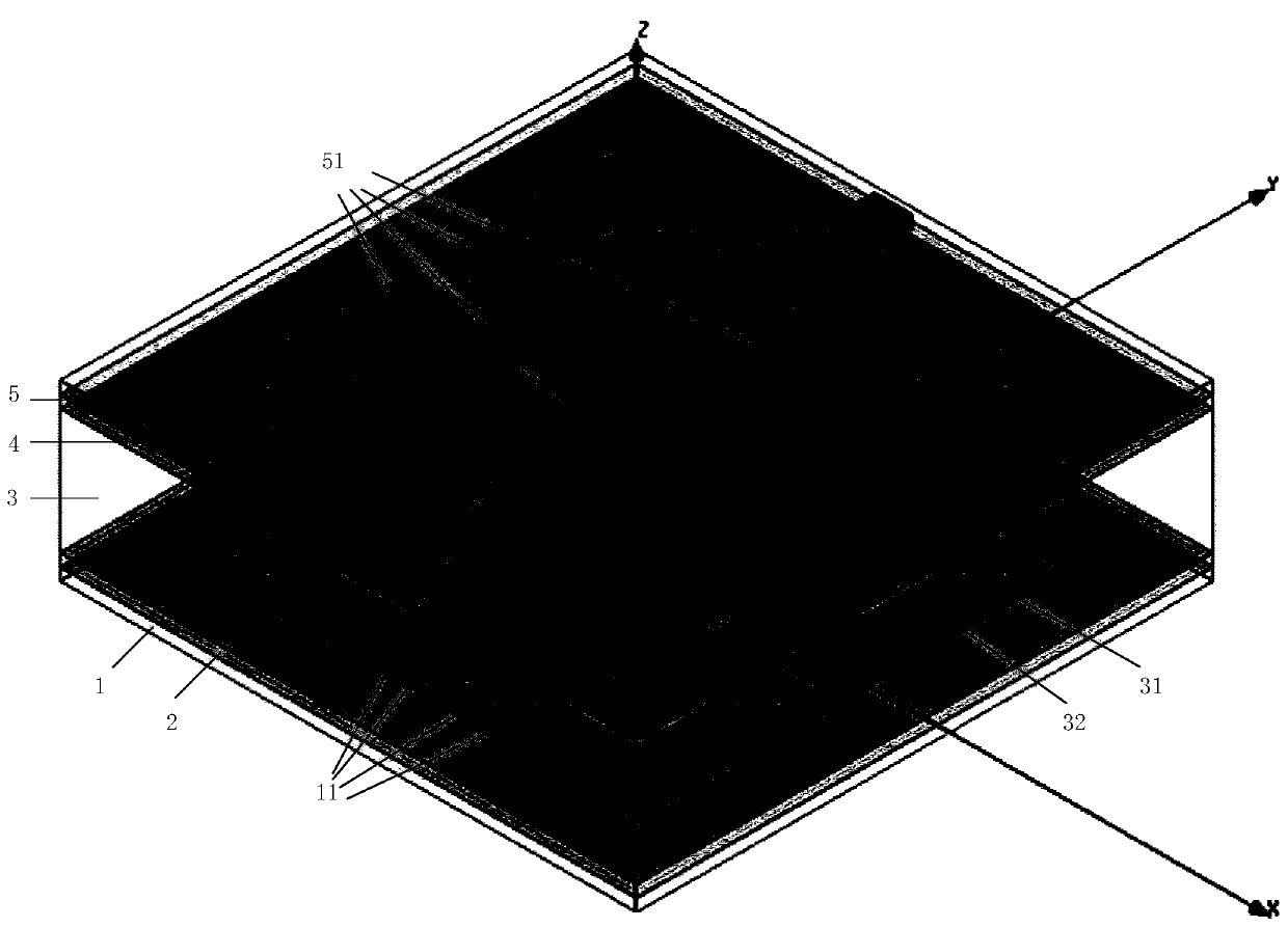
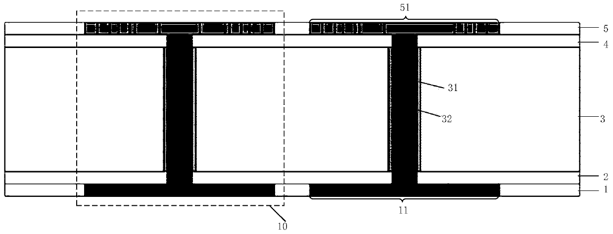
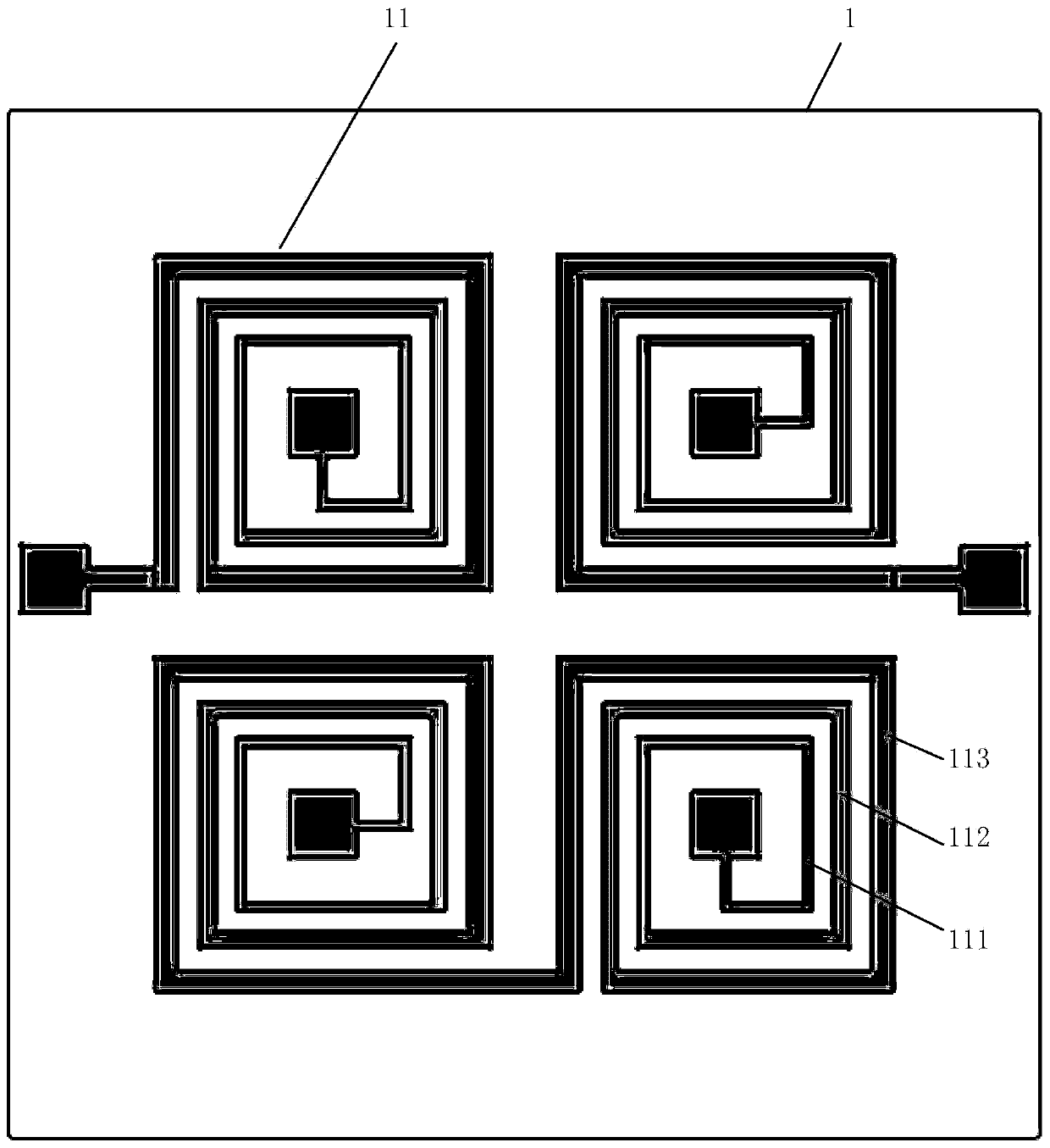
[0036] See figure 1 and figure 2 , figure 1 A schematic structural diagram of a high-density three-dimensional integrated spiral inductor based on through-silicon via interconnection provided by an embodiment of the present invention, figure 2 A cross-sectional view of a high-density three-dimensional integrated spiral inductor based on through-silicon via interconnection provided for an embodiment of the present invention, including: a first metal layer 1 including several first spiral inductors 11; a first dielectric layer 2, Located on the first metal layer 1; the semiconductor substrate 3 is located on the first dielectric layer 2, and a plurality of through holes are arranged in the semiconductor substrate 3, and a dielectric ring 31 and a metal column 32 are arranged in the through holes, and the dielectric ring 31 is located on the Between the metal pillar 32 and the semiconductor substrate 3; the second dielectric layer 4 is located on the semiconductor substrate 3...


PUM

PropertyMeasurementUnit
thicknessaaaaaaaaaa
thicknessaaaaaaaaaa
diameteraaaaaaaaaa

Abstract

The present invention relates to a high-density three-dimensional integrated spiral inductor based on mutual connection of silicon through holes. The inductor comprises: a first metal layer comprisinga plurality of first spiral sub inductors; a first dielectric layer located on the first metal layer; a semiconductor substrate located on the first dielectric layer and internally provided with a plurality of through holes, wherein the through holes are internally provided with dielectric rings and metal columns, the dielectric rings are located between the metal columns and the semiconductor substrate, and the metal columns penetrate the first dielectric layer and are connected with the first spiral sub inductors; a second dielectric layer located on the semiconductor substrate, wherein themetal columns penetrate the second dielectric layer; and a second metal layer located on the second dielectric layer and comprising a plurality of second spiral sub inductors which are connected withthe metal columns, wherein the first spiral sub inductors, the metal columns and the second spiral sub inductors form three-dimensional spiral inductors, and the plurality of sets of the three-dimensional spiral inductors are connected in order. The three-dimensional integrated spiral inductor is simple in structure, high in chip utilization rate, small in size, high in magnetic density, low in process difficulty and low in cost.

Description

technical field [0001] The invention belongs to the field of three-dimensional integrated microwave filters, and in particular relates to a high-density three-dimensional integrated spiral inductor based on through-silicon hole interconnection. Background technique [0002] Inductors are one of the basic components in modern communication systems and are widely used in various unit circuits and systems. With the development of various designs and process technologies, various active devices are shrinking year by year in accordance with Moore's Law, which promotes the continuous reduction in the size of integrated circuits and even electronic systems, and the increasing number of integrated functions. However, passive components such as inductors and capacitors However, the reduction range of devices is far behind, and has gradually become the main bottleneck in the development of miniaturization and integration of electronic communication systems. [0003] According to elec...

Claims


Application Information

Patent Timeline
Patent Type & Authority Applications(China)
IPC IPC(8): H01L23/522H01L23/48H01F17/00H01F27/28H01F27/32
Inventor 尹湘坤朱樟明杨银堂李跃进丁瑞雪
Owner XIDIAN UNIV
Why Eureka
Try Eureka