Spinning light-emitting diode based on Fe3N/GaN heterostructure and preparation method of spinning light-emitting diode
A technology of light-emitting diodes and heterostructures, applied in electrical components, circuits, semiconductor devices, etc., can solve the problems of conductance mismatch and low spin injection efficiency, and achieve the effect of improving efficiency
- Summary
- Abstract
- Description
- Claims
- Application Information
AI Technical Summary
Problems solved by technology
Method used
Image
Examples
Embodiment Construction
[0014] The technical solution of the present invention will be further described in detail below in conjunction with the accompanying drawings.
[0015] Based on Fe 3 Spin light-emitting diode with N / GaN heterostructure and its preparation method, wherein:
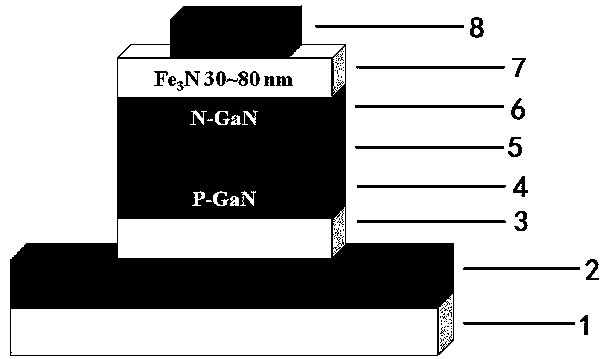
[0016] The spin light emitting diode, refer to figure 1 , its structure includes from bottom to top: substrate 1, bonding layer 2, P electrode 3, P-GaN layer 4, active layer 5, N-GaN layer 6, Fe 3 N film layer 7, electrode 8.
[0017] The preparation method comprises the steps of:
[0018] In step 1, a commercial GaN-based ordinary light-emitting diode is used as a background diode, and its structure includes a substrate 1 , an adhesive layer 2 , a P electrode 3 , a P-GaN layer 4 , an active layer 5 , and an N-GaN layer 6 .
[0019] Step 2, sputtering a layer of (002) oriented Fe on the GaN-based ordinary light-emitting diode in step 1 by magnetron sputtering 3 N film layer 7. Among them, the purity of the iron targe...
PUM
 Abstract
Description
Claims
Application Information
