Preparation method of deep-UV LED

A deep ultraviolet and mask layer technology, applied in the direction of electrical components, circuits, semiconductor devices, etc., can solve the problems of reducing luminous efficiency, loss of quantum well light-emitting layer, and reducing the probability of electron-hole recombination, so as to improve the luminous area, Effect of improving luminous efficiency

Inactive Publication Date: 2019-06-07
SUZHOU HAN HUA SEMICON CO LTD
View PDF4 Cites 3 Cited by
  • Summary
  • Abstract
  • Description
  • Claims
  • Application Information

AI Technical Summary

Problems solved by technology

This nanowire process is obtained by etching on the LED epitaxial wafer structure. Although this structure can improve the light extraction efficiency, it also loses a large area of ​​the quantum well light-emitting layer, and there are a large number of dangling bonds in the etched section. Easy to form non-radiative recombination centers, reducing luminous efficiency
In addition, this nanowire structure does not solve the quantum-confined Stark effect, and the built-in polarization electric field still exists, which reduces the probability of electron-hole recombination, resulting in low internal quantum efficiency.

Method used


Image

  • Preparation method of deep-UV LED
  • Preparation method of deep-UV LED
  • Preparation method of deep-UV LED

Examples


Embodiment Construction

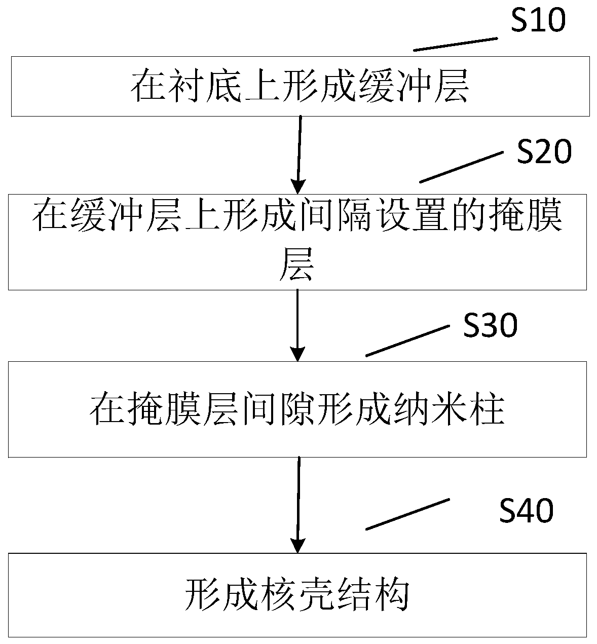
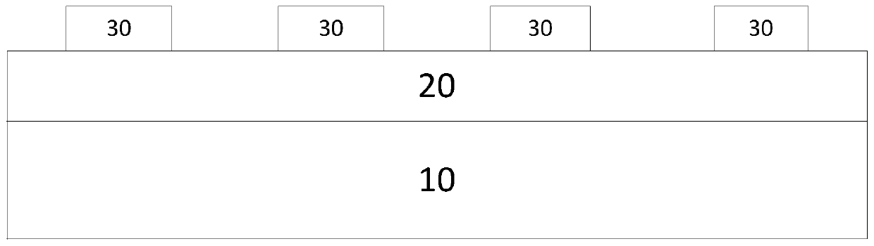
[0024] The preparation method of the deep ultraviolet LED proposed by the present invention will be further described in detail below with reference to the drawings and specific examples. Advantages and features of the present invention will be apparent from the following description and claims. It should be noted that all the drawings are in a very simplified form and use imprecise scales, and are only used to facilitate and clearly assist the purpose of illustrating the embodiments of the present invention.

[0025] In the present invention, in "a layer formed on another layer", it may mean that a layer is formed on another layer, but not necessarily that the layer is in direct physical or electrical contact with another layer (for example, there may be one or more other layers in between). However, in some embodiments, "formed on" may mean that a layer is in direct physical contact with at least a portion of the top surface of another layer.

[0026] Please refer to Fig...


PUM

PropertyMeasurementUnit
thicknessaaaaaaaaaa
thicknessaaaaaaaaaa

Abstract

The present invention provides a preparation method of a deep-UV LED. The preparation method comprises the steps of: providing a substrate, and forming a buffer layer on the substrate; forming mark layers arranged at intervals on the buffer layer; growing n-type AlGaN layers in gaps between the mark layers to form vertically distributed nanorod arrays; and growing a quantum well layer, a p-type AlGaN layer and a p-type GaN layer in order on each n-type AlGaN layer to form core-shell structures comprising the n-type AlGaN layers, the quantum well layers, the p-type AlGaN layers and the p-type GaN layers in order from inside to outside. According to the preparation method of a deep-UV LED, the quantum well layers have large areas compared to a traditional epitaxial structure LED to improve the light emitting area, the light emitting directions of t= most of the quantum well layers are perpendicular to a C surface without being influenced by the quantum-confined stark effect so as to improve the light emitting efficiency.

Description

technical field [0001] The invention relates to the field of LEDs, in particular to a method for preparing a deep ultraviolet LED. Background technique [0002] As a light source, deep ultraviolet LEDs are different from traditional gas deep ultraviolet light sources and mercury deep ultraviolet light sources, and have the advantages of convenience, high efficiency, and environmental protection. High-aluminum component ternary or quaternary nitrides for deep ultraviolet LEDs are the core materials for preparing deep ultraviolet LEDs. However, for a long time, deep ultraviolet LEDs based on high-aluminum component nitrides have been facing problems such as strong absorption of ultraviolet light by inactive materials in LEDs and the quantum-confined Stark effect, resulting in low luminous efficiency of deep ultraviolet LEDs. This greatly restricts the wide application of deep ultraviolet LEDs. [0003] At present, the introduction of nanowires into the LED structure will gre...

Claims


Application Information

Patent Timeline
Patent Type & Authority Applications(China)
IPC IPC(8): H01L33/06H01L33/32H01L33/12H01L33/00
Inventor 华斌何伟
Owner SUZHOU HAN HUA SEMICON CO LTD
Why Eureka
Try Eureka