Infrared-visible light image up-conversion device based on semiconductor quantum dots and liquid crystal, and imaging method
An infrared image and visible light technology, applied in the direction of instruments, optics, measuring devices, etc., can solve the problems that photodetection devices and photoelectric display devices cannot be integrated on the same substrate, and the structure and preparation process are not compatible, so as to achieve low preparation cost, Enhanced photodetection sensitivity and simple device structure
- Summary
- Abstract
- Description
- Claims
- Application Information
AI Technical Summary
Problems solved by technology
Method used
Image

Examples
Embodiment Construction
[0025] The technical solutions of the present invention will be further described below in conjunction with the accompanying drawings and embodiments.
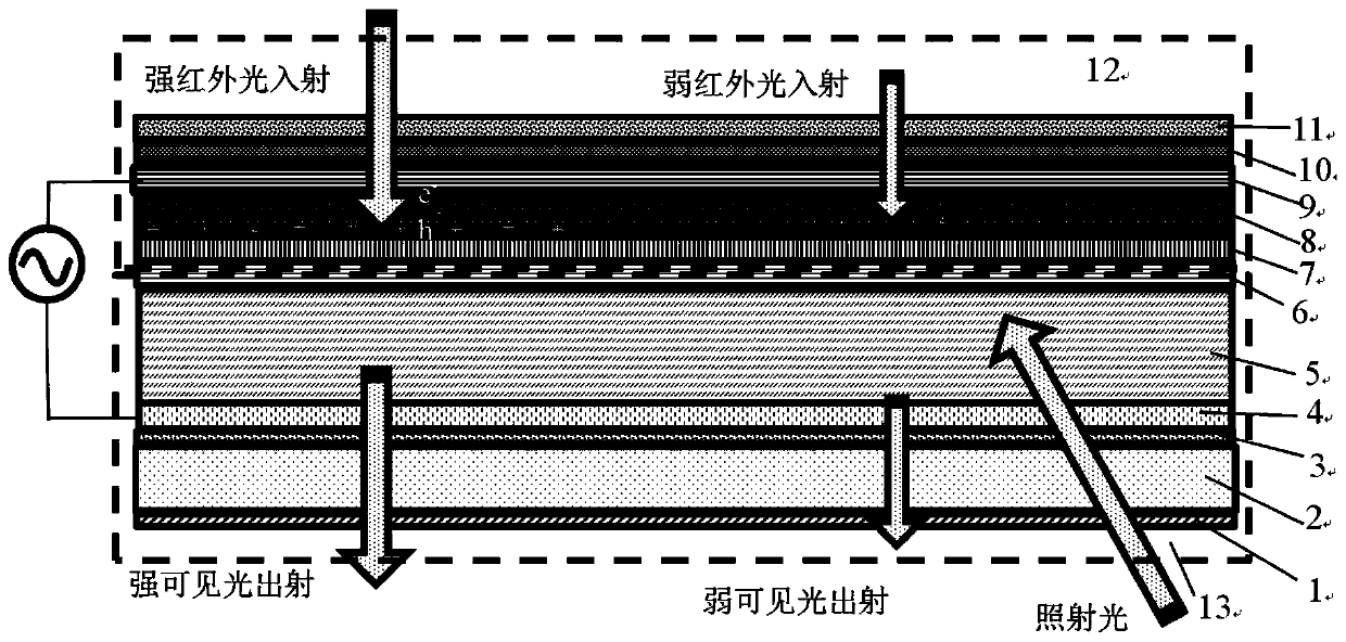
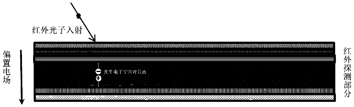
[0026] Such as figure 1 and figure 2 As shown, the infrared-visible light image up-conversion device based on semiconductor quantum dots and liquid crystals of the present invention includes an upper substrate 11, a visible light shielding layer 10, an infrared transparent electrode 9, a semiconductor quantum dot photoelectric active layer 8, and a visible light from top to bottom. Reflective layer 7 , liquid crystal upper alignment layer 6 , liquid crystal layer 5 , liquid crystal lower alignment layer 4 , visible light transparent electrode 3 , lower substrate 2 and polarizer 1 . Among them, 1-6 constitute the visible light image display component 13, which is the visible light image display part based on liquid crystal; 6-11 constitute the infrared image detection component 12, which is the infrared image detection part b...
PUM
 Abstract
Description
Claims
Application Information