Inorganic perovskite thick film composite material semiconductor device and preparation method thereof
A composite material and inorganic calcium technology, which is applied in the manufacture of semiconductor devices, electrical components, and final products, can solve the problem that thin films cannot meet the physical requirements of high-energy particle detection, single crystals cannot be grown on a large scale, large-size, and do not have repeatability, etc. problems, achieve excellent photoelectric response, high repeatability, and improve performance
- Summary
- Abstract
- Description
- Claims
- Application Information
AI Technical Summary
Problems solved by technology
Method used
Image

Examples
Embodiment 1
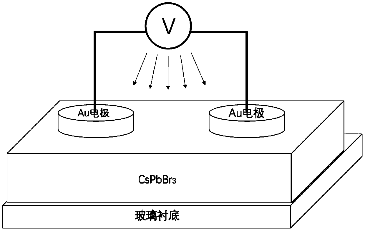
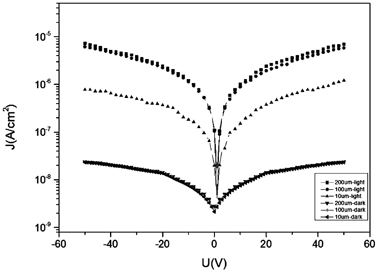
[0035] In this example, see figure 1 , an inorganic perovskite thick-film composite semiconductor device, the transparent glass is used as a substrate with a plane size of 2cm*2cm, and the inorganic perovskite thick-film composite semiconductor device consists of transparent glass, a perovskite light-absorbing layer, a metal The electrode is composed of transparent glass / CsPbBr 3 Composite structure composed of perovskite polycrystalline thick film / Au electrode as an all-inorganic perovskite planar semiconductor detector material, CsPbBr 3 Perovskite polycrystalline thick film as electron hole transport functional layer, CsPbBr 3 The thickness of the perovskite polycrystalline thick film is 10 μm, and the thickness of the Au electrode is 70 nm. The perovskite light-absorbing layer is prepared by a single-step thermal spraying method. The metal electrodes are composed of Au point electrodes. The inorganic perovskite thick-film composite device is used as an X-ray thick-film...
Embodiment 2
[0048] This embodiment is basically the same as Embodiment 1, especially in that:
[0049] In this embodiment, an inorganic perovskite thick-film composite semiconductor device, the transparent glass is used as a substrate with a planar size of 2cm*2cm, and the inorganic perovskite thick-film composite semiconductor device is made of transparent glass, perovskite Composed of mineral light-absorbing layer and metal electrodes, its structure is made of transparent glass / CsPbBr 3 Composite structure composed of perovskite polycrystalline thick film / Au electrode as an all-inorganic perovskite planar semiconductor detector material, CsPbBr 3 Perovskite polycrystalline thick film as electron hole transport functional layer, CsPbBr 3 The thickness of the perovskite polycrystalline thick film is 100 μm, and the thickness of the Au electrode is 80 nm. The perovskite light-absorbing layer is prepared by a single-step thermal spraying method. The metal electrodes are composed of Au po...
Embodiment 3
[0062] This embodiment is basically the same as the previous embodiment, and the special features are:
[0063] In this embodiment, an inorganic perovskite thick-film composite semiconductor device, the transparent glass is used as a substrate with a planar size of 2cm*2cm, and the inorganic perovskite thick-film composite semiconductor device is made of transparent glass, perovskite Composed of mineral light-absorbing layer and metal electrodes, its structure is made of transparent glass / CsPbBr 3Composite structure composed of perovskite polycrystalline thick film / Au electrode as an all-inorganic perovskite planar semiconductor detector material, CsPbBr 3 Perovskite polycrystalline thick film as electron hole transport functional layer, CsPbBr 3 The thickness of the perovskite polycrystalline thick film is 200 μm, and the thickness of the Au electrode is 90 nm. The perovskite light-absorbing layer is prepared by a single-step thermal spraying method. The metal electrodes a...
PUM
| Property | Measurement | Unit |
|---|---|---|
| thickness | aaaaa | aaaaa |
| thickness | aaaaa | aaaaa |
| thickness | aaaaa | aaaaa |
Abstract
Description
Claims
Application Information
 - R&D
- Intellectual Property
- Life Sciences
- Materials
- Tech Scout
- Unparalleled Data Quality
- Higher Quality Content
- 60% Fewer Hallucinations
Browse by: Latest US Patents, China's latest patents, Technical Efficacy Thesaurus, Application Domain, Technology Topic, Popular Technical Reports.
© 2025 PatSnap. All rights reserved.Legal|Privacy policy|Modern Slavery Act Transparency Statement|Sitemap|About US| Contact US: help@patsnap.com