
Preparation method of Gan-based light-emitting diode epitaxial wafer

A technology of light-emitting diodes and epitaxial wafers, applied in semiconductor/solid-state device manufacturing, semiconductor devices, electrical components, etc., can solve the problem of low hole concentration in the P-type GaN layer, reduce the formation of Mg-H complexes, and avoid Effect of non-radiative recombination and high crystal growth quality

Active Publication Date: 2021-10-01
HC SEMITEK ZHEJIANG CO LTD
View PDF4 Cites 0 Cited by
  • Summary
  • Abstract
  • Description
  • Claims
  • Application Information

AI Technical Summary

Problems solved by technology

The P-type GaN layer grown in this way has a lower hole concentration

Method used


Image

  • Preparation method of Gan-based light-emitting diode epitaxial wafer
  • Preparation method of Gan-based light-emitting diode epitaxial wafer

Examples


Embodiment Construction

[0021] In order to make the objects, technical solutions, and advantages of the present invention, the embodiments of the present invention will be further described in detail below with reference to the accompanying drawings.

[0022] In the relevant technique, the P-type GaN layer adopts N 2 Ho 2 The mixed gas is used as a carrier gas, since Mg is required in the p-type GaN layer to produce sufficient holes, but the MG is soluble in GaN low, easy to form Mg-H complexes with h, which caused by deep levels caused by these complexes Receptors will cause non-radiation complications caused by the hole trap to reduce the concentration of the hole. In addition, the H atom is small, the Mo (Metalorganic Source, Metal Organic Organic Source) is less; the N atom is large, and the Mo brought into. Mo is a high-purity metal organic compound material, which is a metal organic chemical gas phase epitaxial and deposited raw materials. When the B-type GaN layer is not high, the voltage of the L...


PUM

PropertyMeasurementUnit
thicknessaaaaaaaaaa
thicknessaaaaaaaaaa
thicknessaaaaaaaaaa

Abstract

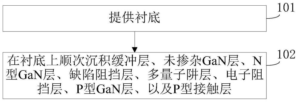
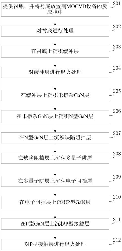
The invention discloses a method for preparing GaN-based light-emitting diode epitaxial wafers, belonging to the field of GaN-based light-emitting diodes. The method includes: providing a substrate; sequentially depositing a buffer layer, an undoped GaN layer, an N-type GaN layer, a defect blocking layer, a multi-quantum well layer, an electron blocking layer, a P-type GaN layer, and a P-type contact layer, the P-type GaN layer includes a first GaN sublayer and a second GaN sublayer, the first GaN sublayer is located between the electron blocking layer and the second GaN sublayer, and When depositing the first GaN sublayer, use N 2 and H 2 The mixed gas is used as the carrier gas, and when depositing the second GaN sublayer, N 2 as a carrier gas.

Description

Technical field [0001] The present invention relates to the field of GaN-based air optical diodes, and more particularly to a method of preparing a GaN-based transmitted emitting diode epitaxial sheet. Background technique [0002] GaN (gallium nitride) based LED (Light Emitting Diode, LED), also known as GaN-based LED chip, typically includes an epitaxial piece and an electrode prepared on an epitaxial sheet. The epitaxial sheet generally includes: a substrate, and a GaN-based extension layer grown on the substrate. The GaN-prolapsed layer includes a sequentially laminated buffer layer, an undoped GaN layer, an N-type GaN layer, MQW (Multiplequantum Well, Multi-quantum well) layer, an electron blocking layer, a p-type GaN layer, and a contact layer. When there is a current injecting the GaN-based LED, the electron and the hole of the N-type region of the n-type GaN layer and the pockets of the P-type region such as the P-type GaN layer enter the MQW active region and composite, ...

Claims


Application Information

Patent Timeline
Patent Type & Authority Patents(China)
IPC IPC(8): H01L21/205H01L21/67H01L33/00
Inventor 曹阳乔楠王群郭炳磊吕蒙普胡加辉李鹏
Owner HC SEMITEK ZHEJIANG CO LTD
Learn More