Large-size chip system package structure with flexible adapter plate and manufacturing method thereof

A chip system and packaging structure technology, applied in semiconductor/solid-state device manufacturing, semiconductor/solid-state device components, semiconductor devices, etc., can solve problems such as unfavorable signal transmission and data processing, large system size, and inability to meet packaging requirements. , to avoid the height difference of solder balls

Active Publication Date: 2019-06-18
INST OF MICROELECTRONICS CHINESE ACAD OF SCI
View PDF6 Cites 1 Cited by
  • Summary
  • Abstract
  • Description
  • Claims
  • Application Information

AI Technical Summary

Problems solved by technology

Processing requirements After the SMT nozzle is installed, the chip bonding surface must be controlled to be parallel to the substrate. On the one hand, a large-size chip corresponds to a large-size flip-chip soldering tool, which is very difficult to manufacture. On the other hand, if a large-size chip has a small Tilt, even a small inclination will cause one side of the chip to touch the substrate and the other side will have a larger distance from the substrate. This distance will lead to virtual soldering. For example, a distance of more than 1mm will lead to virtual soldering, and even some solder balls cannot be soldered at all. onto the substrate
In addition, the substrate must not have any warping during the placement process, as warping will also lead to virtual soldering and even some solder balls cannot be soldered
Conventional patch + reflow process, during the reflow process, when the substrate is transferred from the low temperature to the high temperature area, due to the vibration and uneven heating of the substrate, the small warping deformation of the large-size substrate will cause the diagonal of the large-size chip The upper end produces millimeter-level warpage, and the solder balls are usually only a few hundred microns in diameter. Therefore, a large number of solder balls will be soldered or even a large number of solder balls cannot be soldered.
Similarly, if in-situ patch reflow soldering is used, since the heating is through the suction head and the substrate platform, the temperature distribution on the upper and lower surfaces of the substrate is very uneven, causing the substrate to still warp, and the same false soldering cannot be avoided
[0004] Secondly, the heat dissipation of large-size chips is an important issue. Heat dissipation during the operation of large-size chips is an important issue for large-size chip packaging. Conventional packaging has a heat sink attached to the back of the chip. For large-size packaging, it has higher heat dissipation requirements. Only relying on a single-sided heat sink cannot meet the heat dissipation requirements
[0005] Therefore, there are still the following technical problems to be solved urgently: large-size chips are packaged using the existing flip-chip soldering technology, which will cause virtual soldering and cannot meet the packaging requirements; Heat dissipation requirements; an independent large-size chip package occupies too much space, resulting in an oversized system with a large-size chip package, which is not conducive to signal transmission and data processing

Method used


Image

  • Large-size chip system package structure with flexible adapter plate and manufacturing method thereof
  • Large-size chip system package structure with flexible adapter plate and manufacturing method thereof
  • Large-size chip system package structure with flexible adapter plate and manufacturing method thereof

Examples


Embodiment Construction

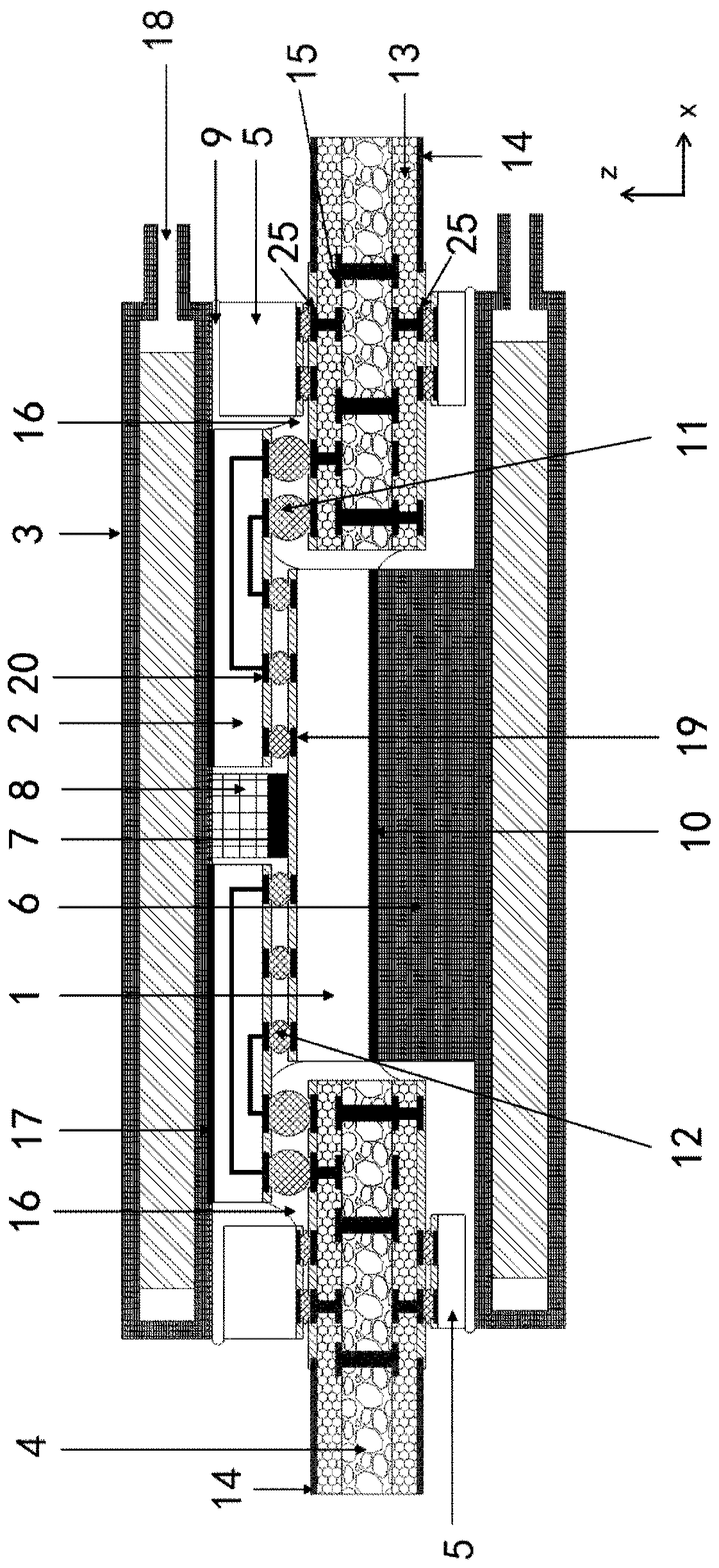
[0060] The present disclosure provides a large-size system-on-chip packaging structure with a flexible interposer. The large-scale system-on-a-chip package structure with a flexible interposer avoids virtual soldering of large-sized chips or other poor soldering problems while ensuring The heat dissipation effect is good. Of course, the large-size chip system packaging structure with a flexible interposer of the present disclosure can be used to simultaneously package one or more large-size chips and / or small-size chips, as well as multiple components. The components can be It is a flip-chip or other type of components, which realizes the packaging and heat dissipation of system functions, and avoids the problem of virtual soldering of large-size chips.

[0061] to combine figure 1 , Figure 7 and Figure 13 As shown, the large-scale chip system packaging structure with a flexible interposer of the present disclosure includes: a flexible interposer 2, which is provided with ...


PUM

PropertyMeasurementUnit
Thicknessaaaaaaaaaa

Abstract

The invention discloses a large-size chip system package structure with a flexible adapter plate, and a manufacturing method thereof. The structure comprises the flexible adapter plate with a first window; a first chip, wherein radiating structures are arranged on a front and a back of the first chip, and the first chip is arranged on the flexible adapter plate in an inversion way and electricallyand mutually connected with the flexible adapter plate, and the radiating structure on the front of the first chip is embedded into the first window; a substrate with a second window, wherein the first chip is arranged on the flexible adapter plate in the inversion way to form a first structure, the first structure is arranged in the second window of the substrate in the inversion way, the firstchip and the radiating structure on the back thereof are embedded into the second window, and the flexible adapter plate is fixed on the substrate and electrically connected with the same; componentsfixed on substrate surface bonding pads at an upper surface and a lower surface of the substrate; and radiators arranged at the back of the flexible adapter plate and the back of the substrate. The reliability of each of the radiating and the package is guaranteed when the cold joint is avoided, the package volume is greatly reduced, the signal transmission path si reduced, and the loss is reduced.

Description

technical field [0001] The disclosure belongs to the technical field of chip packaging, and relates to a large-size chip system packaging structure with a flexible adapter plate and a manufacturing method thereof. Background technique [0002] With the continuous development of semiconductor technology, the system on chip (SOC, System on a chip) technology has been developed unprecedentedly. More and more transistors are integrated on the SOC chip, and the functions are becoming more and more powerful. Due to the increase in the number of transistors, the size of the SOC chip It is getting bigger and bigger, and the conventional SOC chip of 1 cm x 1 cm to 2 cm x 2 cm can no longer meet the requirements. At present, it has developed to a chip of 3-4 cm square, and will reach and break through 5 cm x 5 cm in the future. For the packaging of large-size chips, there are great difficulties in packaging technology. [0003] First of all, in order to meet the performance requireme...

Claims


Application Information

Patent Timeline
IPC IPC(8): H01L23/498H01L23/367H01L21/48H01L21/60H01L21/683
CPCH01L2224/16225H01L2924/15151H01L2924/15192
Inventor 于中尧
Owner INST OF MICROELECTRONICS CHINESE ACAD OF SCI
Why Eureka
Try Eureka