MOSFET device

A device and trench technology, applied in semiconductor devices, electrical components, circuits, etc., can solve problems such as poor reliability of gate dielectrics, achieve low on-resistance and gate-to-drain capacitance, and improve reliability and life.

Active Publication Date: 2019-06-21
INST OF SEMICONDUCTORS - CHINESE ACAD OF SCI +1
View PDF4 Cites 8 Cited by
  • Summary
  • Abstract
  • Description
  • Claims
  • Application Information

AI Technical Summary

Problems solved by technology

At the same time, there is a phenomenon of electric field concentration at the bottom of the trench (8

Method used


Image

  • MOSFET device
  • MOSFET device
  • MOSFET device

Examples


Embodiment Construction

[0023] In order to make the purpose, features and advantages of the present invention more obvious and understandable, the technical solutions in the embodiments of the present invention will be clearly and completely described below in conjunction with the accompanying drawings in the embodiments of the present invention. Obviously, the described The embodiments are only some of the embodiments of the present invention, but not all of them. Based on the embodiments of the present invention, all other embodiments obtained by those skilled in the art without making creative efforts belong to the protection scope of the present invention.

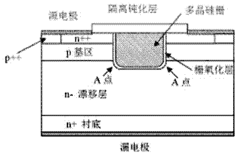
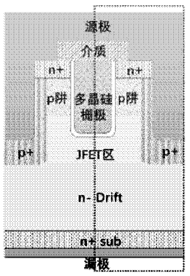
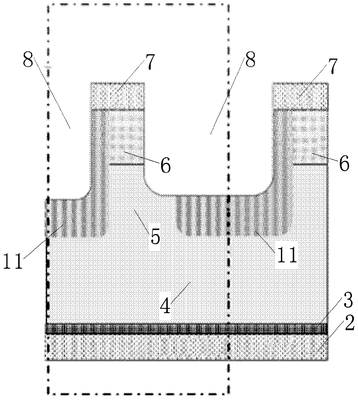
[0024] The n-type doping and p-type doping mentioned in the embodiment of the present invention are relative terms, and can also be referred to as the first doping and the second doping, that is, the interchange of n-type and p-type is also applicable to devices . At the same time, the device structure in the embodiment of the present invent...


PUM

PropertyMeasurementUnit
Thicknessaaaaaaaaaa

Abstract

The invention discloses an MOSFET device, which is applied to the technical field of semiconductors. A primitive cell structure of an active region of the MOSFET device comprises a drain electrode (1), an n+ substrate (2), an n-type buffer layer (3), an n-drift region (4), an n-type JFET region (5), a P base region (6) and an n+ layer (7) in sequence from bottom to top; the primitive cell structure of the active region of the MOSFET device is an asymmetric structure; a groove (8) is formed in the primitive cell structure; one side of the groove (8) is provided with a gate dielectric (9) and apolysilicon gate electrode (10), and the other side of the groove (8) is provided with a P+ region (11) and a source electrode (12); and the polysilicon gate electrode (10) and the source electrode (12) are isolated by a dielectric layer (13). The structure of the device can effectively shield an electric field of the gate dielectric at the bottom of the groove (8), so that the reliability and theservice life of the device are improved and prolonged, and meanwhile, low on resistance and gate-drain capacitance are obtained.

Description

technical field [0001] The invention relates to the technical field of semiconductors, in particular to a MOSFET device. Background technique [0002] SiC trench (8) MOSFET (TMOS) has many advantages, such as p well (or called P base region (6)) can be formed by epitaxial growth, which eliminates the influence of defects when ion implantation forms p well, and has a more Good MOS gate quality and channel mobility, and easier control of channel length. At the same time, since the conduction channel is on (11-20), (1.100) or other crystal planes, the channel mobility is more than twice that of the planar MOSFET (0001) plane, and the on-resistance can be further reduced. In addition, the primary cell (basic unit constituting the active region of the device) of the trench (8) type MOSFET can be made smaller, and the higher primary cell density can further reduce the on-resistance. However, since the critical electric field strength of SiC is about 10 times that of Si, and SiO ...

Claims


Application Information

Patent Timeline
IPC IPC(8): H01L29/78H01L29/06H01L29/08H01L29/167H01L29/423
Inventor 王晓亮倪炜江冯春肖红领姜丽娟李巍王权
Owner INST OF SEMICONDUCTORS - CHINESE ACAD OF SCI
Why Eureka
Try Eureka