An MEMS bridge structure and a forming method thereof

A technology of bridge structure and laminated structure, which is applied in the direction of microstructure technology, microstructure device, manufacturing microstructure device, etc., can solve the problems of bridge warpage, affecting packaging and testing, etc., and achieve the goal of reducing bridge warpage and preventing bridge warpage Effect

Inactive Publication Date: 2019-06-25
SHANGHAI HUAHONG GRACE SEMICON MFG CORP
View PDF9 Cites 3 Cited by
  • Summary
  • Abstract
  • Description
  • Claims
  • Application Information

AI Technical Summary

Problems solved by technology

[0004] In view of the above-mentioned shortcomings of the prior art, the object of the present invention is to provide a MEMS bridge structure and its forming method, which is used to solve the bridge warpage caused by the release of the MEMS bridge structure in the prior art, thereby affecting the quality of subsequent packaging tests. question

Method used


Image

  • An MEMS bridge structure and a forming method thereof
  • An MEMS bridge structure and a forming method thereof
  • An MEMS bridge structure and a forming method thereof

Examples


Embodiment 1

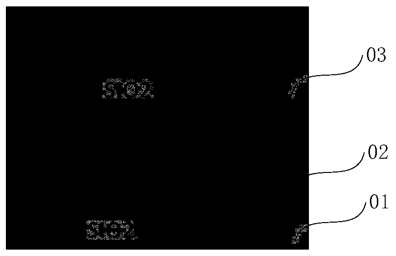
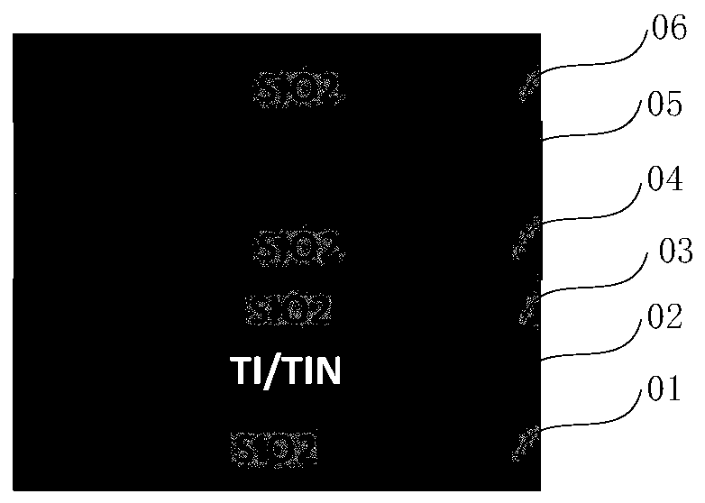
[0027] refer to figure 2 , figure 2 Shown is a schematic diagram of the MEMS bridge structure layer of the present invention. The MEMS bridge structure is characterized in that it at least includes: a substrate 01; a titanium-containing thin film layer 02 located on the substrate 01; a silicon oxide thin film layer 03 located on the titanium-containing thin film layer 02; Composite film layer on film layer 03. Preferably in the present invention, the substrate is a silicon substrate, or a silicon dioxide film layer or an amorphous silicon film layer. In this embodiment, preferably, the substrate is a silicon dioxide film layer. In this embodiment, preferably, the titanium-containing thin film layer 02 on the substrate 01 contains titanium and titanium nitride, that is, the titanium-containing thin film layer 02 is composed of a mixture of titanium and titanium nitride. Further, the thickness of the titanium-containing thin film layer is 100 angstroms to 200 angstroms. F...

Embodiment 2

[0035] refer to figure 2 , figure 2 Shown is a schematic diagram of the MEMS bridge structure layer of the present invention. The MEMS bridge structure is characterized in that it at least includes: a substrate 01; a titanium-containing thin film layer 02 located on the substrate 01; a silicon oxide thin film layer 03 located on the titanium-containing thin film layer 02; Composite film layer on film layer 03. Preferably in the present invention, the substrate is a silicon substrate, or a silicon dioxide film layer or an amorphous silicon film layer. In this embodiment, preferably, the substrate is a silicon dioxide film layer.

[0036] The difference between the second embodiment and the first embodiment is that the titanium-containing film layer 02 on the substrate 01 is a titanium nitride film layer, that is to say, the titanium-containing film layer 02 is only composed of a titanium nitride material constitute. Further, the thickness of the titanium-containing thin fi...


PUM

PropertyMeasurementUnit
thicknessaaaaaaaaaa
thicknessaaaaaaaaaa
thicknessaaaaaaaaaa

Abstract

The invention provides an MEMS bridge structure and a forming method thereof. The MEMS bridge structure comprises a substrate and a titanium-containing thin film layer located on the substrate, a silicon oxide film layer located on the titanium-containing film layer, and a composite film layer located on the silicon oxide film layer. The forming method of the MEMS bridge structure comprises the steps that a substrate is provided, and a titanium-containing thin film layer is formed on the substrate; a silicon oxide film layer is formed on the titanium-containing film layer; and a composite filmlayer is formed on the silicon oxide film layer. The stress of several films is neutralized by controlling the stress of the bridge structure: the films with multiple reaction stresses are added to be applied to the process with the bridge structure in the MEMS process, so that the bridge warpage caused by release of the bridge structure can be effectively reduced, and the subsequent packaging test is influenced. The thickness of the whole bridge structure is not affected, and meanwhile alignment of the follow-up photoetching process and control over a follow-up etching channel are facilitated. Due to the adoption of various composite films, the stress of the films is neutralized by the multilayer films, and the bridge is prevented from warping.

Description

technical field [0001] The invention relates to the field of semiconductor integrated circuit manufacturing, in particular to a MEMS bridge structure and a forming method thereof. Background technique [0002] Warping of semiconductor wafers occurs during the manufacturing process and later when electronic components and circuits are fabricated on the wafer. Warpage, also known as bending, refers to the phenomenon that the wafer is deformed and uneven in the semiconductor field. Warpage will affect the quality of the wafer and the progress of the semiconductor manufacturing process. For example, during the photoetching process, if the wafer is deformed, the illuminated surface will be uneven, which will cause the mask structure to fail to form a clear image, thus affecting the etching process. Eclipse precision. Amorphous silicon is an allotropic form of silicon that can be deposited in thin films on a variety of substrates, providing certain unique functionalities for a v...

Claims


Application Information

Patent Timeline
Patent Type & Authority Applications(China)
IPC IPC(8): B81B7/02B81C1/00
Inventor 刘善善朱黎敏
Owner SHANGHAI HUAHONG GRACE SEMICON MFG CORP
Why Eureka
Try Eureka