Spherical box-shaped three-dimensional detector and preparation method thereof
A detector and box-shaped technology, which is applied in the field of spherical box-shaped three-dimensional detectors and its preparation, can solve the problems of poor charge collection efficiency of three-dimensional grooved silicon detectors, reduced energy resolution of three-dimensional grooved silicon detectors, central column The surface area distribution of the shape electrode is long and other problems, and the internal electric field distribution is uniform, the overall size is small, and the response time is short.
- Summary
- Abstract
- Description
- Claims
- Application Information
AI Technical Summary
Problems solved by technology
Method used
Image
Examples
Embodiment 1
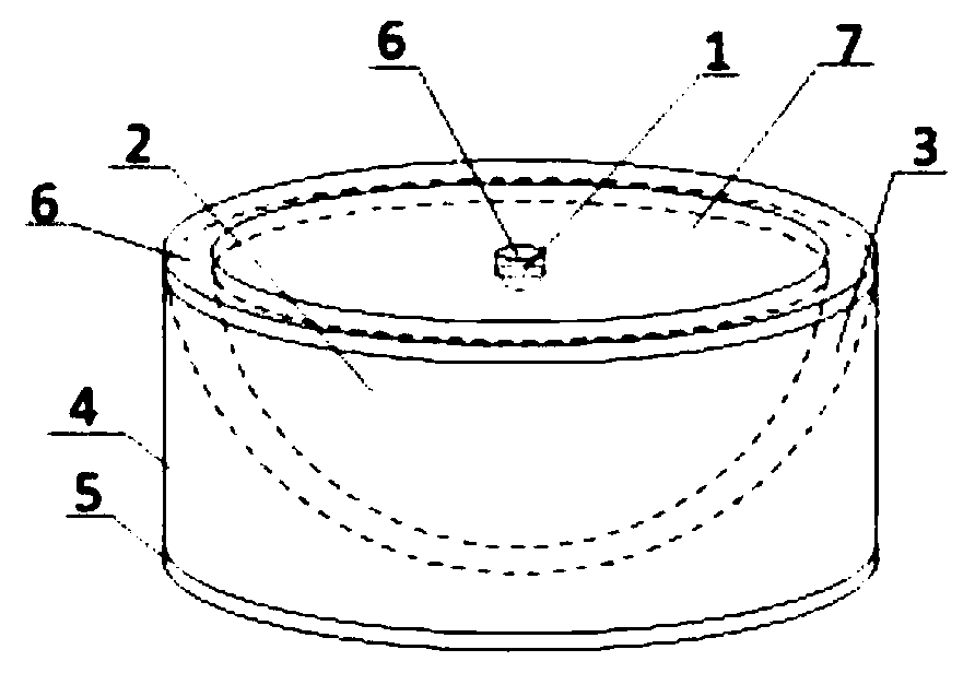
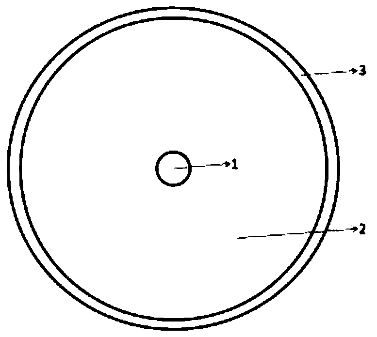
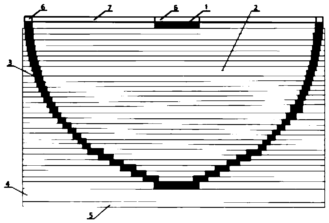
[0047] The semiconductor substrate 2 is an N-type semiconductor material, the central collecting electrode 1 is an N-type heavily doped semiconductor material, and the shell-shaped electrode 3 is a P-type heavily doped semiconductor material, wherein the doping concentration of the semiconductor substrate 2 is 1×10 12 cm -3 , the doping concentration of the central collecting electrode 1 is 1×10 18 cm -3 , the doping concentration of shell electrode 3 is 5×10 19 cm -3 , the preparation process is as follows:
[0048] Step 1: Attach a 1 μm thick N-type lightly doped material on a 1 μm thick N-type high-resistance silicon chip to form a substrate 4;
[0049] Step 2: Ion-implanting a cylindrical P-type heavily doped semiconductor material with a height of 1 μm and a cross-sectional radius of 1 μm on the substrate 4;
[0050] Step 3: Grow cylindrical N-type lightly doped silicon with a thickness of 1 μm on the wafer, and the bottom surface of the N-type lightly doped silicon ...
Embodiment 2
[0056] In the case of the same doping type in Embodiment 1, the doping concentration of the semiconductor base 2 is 1×10 12 cm -3 , the doping concentration of the central collecting electrode 1 is 5×10 19 cm -3 , the doping concentration of shell electrode 3 is 1×10 18 cm -3 .
Embodiment 3
[0058] In the case of the same doping type in Embodiment 1, the doping concentration of the semiconductor base 2 is 1×10 12 cm -3 , the doping concentration of the central collecting electrode 1 is 2.45×10 19 cm -3 , the doping concentration of shell electrode 3 is 2.45×10 19 cm -3 .
[0059] The boundary condition of the detector described in embodiments 1-3 is: The Poisson equation is: Available:
[0060]
[0061] where |V|≤V fd , r 1 ≥r c , when fully depleted, r 1 = r c ,
[0062]
[0063] is the potential at the edge of the depletion layer of the PN junction in the detection unit, is the potential at any point in the detection unit, is the potential at the outer edge of the shell-shaped electrode 3 of the detection unit, |V| the absolute value of the applied voltage difference, r 1 is the distance between any point in the detection unit and the center of the central collecting electrode 1, R is the distance between the center of the central co...
PUM
 Abstract
Description
Claims
Application Information


