GaInP/GaAs/InGaAs three-junction film solar cell

A thin-film solar cell and battery technology, applied in the field of solar cells, can solve problems such as cell gaps, and achieve the effects of reducing defect density, reducing compound current, and increasing short-circuit current.

Pending Publication Date: 2019-06-28
DR TECH CO LTD YIXING JIANGSU
View PDF0 Cites 3 Cited by
  • Summary
  • Abstract
  • Description
  • Claims
  • Application Information

AI Technical Summary

Problems solved by technology

[0003] The traditional design of the three sub-cells of the GaInP/GaAs/InGaAs triple-junction thin-film solar cell is to use the n-type heavily doped emitter region above the base region (light-inciden

Method used


Image

  • GaInP/GaAs/InGaAs three-junction film solar cell
  • GaInP/GaAs/InGaAs three-junction film solar cell
  • GaInP/GaAs/InGaAs three-junction film solar cell

Examples


Embodiment 1

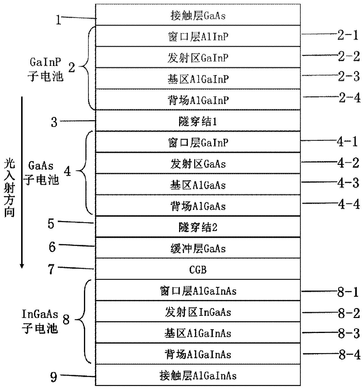
[0053] An N-type GaAs substrate is used as a substrate, on which an AlAs lift-off sacrificial layer is epitaxially grown, and then layers 1 to 9 are epitaxially grown in sequence. in:

[0054] The GaInP top cell window layer is made of Si-doped AlInP with a doping concentration of 1x10 18 cm -3 , with a thickness of 30nm; the emission region is made of Si-doped GaInP with a doping concentration of 5x10 17 cm -3 , with a thickness of 500nm; the base region is made of Zn-doped Al 0.15 GaInP with a doping concentration of 2x10 18 cm -3 , the thickness is 50nm; the back field uses Zn-doped AlGaInP, the thickness is 50nm, the Al composition in the material increases linearly from 0.15 to 0.25 from the interface of the base region, and the doping concentration increases from 1x10 18 cm -3 Exponent increased to 5x10 18 cm -3 .

[0055] The cell window layer in GaAs is made of Si-doped GaInP with a doping concentration of 2x10 18 cm -3 , with a thickness of 30nm; the emiss...

Embodiment 2

[0060] An N-type GaAs substrate is used as a substrate, on which an AlAs lift-off sacrificial layer is epitaxially grown, and then layers 1 to 9 are epitaxially grown in sequence. in:

[0061] The GaInP top cell window layer is made of Si-doped AlInP with a doping concentration of 1x10 18 cm -3 , with a thickness of 30nm; the emission region is made of Si-doped GaInP with a doping concentration of 2x10 17 cm -3 , with a thickness of 700nm; the base region is made of Zn-doped Al 0.25 GaInP with a doping concentration of 2x10 18 cm -3 , the thickness is 50nm; the back field adopts Zn-doped AlGaInP, the thickness is 50nm, the Al composition in the material increases linearly from 0.25 to 0.5 from the interface of the base region, and the doping concentration increases from 1x10 18 cm -3 Exponent increased to 3x10 18 cm -3 .

[0062] The cell window layer in GaAs is made of Si-doped GaInP with a doping concentration of 2x10 18 cm -3 , with a thickness of 30nm; the emis...


PUM

PropertyMeasurementUnit
Thicknessaaaaaaaaaa
Thicknessaaaaaaaaaa
Thicknessaaaaaaaaaa

Abstract

The invention provides a GaInP/GaAs/InGaAs three-junction film solar cell which comprises a GaInP top cell, a GaAs intermediate cell and an InGaAs bottom cell successively along the light incident direction. The GaInP top cell and GaAs intermediate cell are provided with a first tunneling junction; and a second tunneling junction and a crystal graded buffer (CGB) layer is arranged between the GaAsintermediate cell and InGaAs bottom cell successively. Each of the GaInP top cell, GaAs intermediate cell and InGaAs bottom cell uses an nP+ heterojunction structure, and compared with a traditionalGaInP/GaAs/InGaAs three-junction film solar cell with an N+p structure, the area of metal grids in the surface of the GaInP top cell is reduced, influence of CGB defect on the material quality of thepn junction region of the InGaAs bottom cell is reduced, the short circuit current Jsc and the open circuit voltage Voc of the cell are improved effectively, and the conversion efficiency is higher.

Description

technical field [0001] The present disclosure relates to the field of solar cells, in particular to a structural design of a GaInP / GaAs / InGaAs triple-junction thin-film solar cell. Background technique [0002] III-V compound semiconductor solar cells represented by GaAs can be prepared into thin-film cells by epitaxy and post-exfoliation method. Compared with Ge-based / Si-based solar cells, they have higher power / mass ratio and flexible and bendable advantages. It has irreplaceable advantages in application fields such as aerospace, long-stay drones, and portable power supplies. Theoretically, III-V compound solar cells can be designed into various structures of 1~n junction (n>4), but from the perspective of efficiency / cost ratio, GaInP / GaAs / InGaAs triple-junction thin-film solar cells are currently the most widely used solar cells. One of many structures. [0003] The traditional design of the three sub-cells of the GaInP / GaAs / InGaAs triple-junction thin-film solar ce...

Claims


Application Information

Patent Timeline
IPC IPC(8): H01L31/0304H01L31/0445H01L31/0735
CPCY02E10/544
Inventor 朱明星吴慧哲李华王伟明
Owner DR TECH CO LTD YIXING JIANGSU
Why Eureka
Try Eureka