Multifunctional processing device for printed circuit board

A technology for printed circuit boards and processing devices, which is applied in the field of processing devices for printed circuit boards. It can solve the problems of inconvenient magnifying lens wiping, inconvenient application of solder paste, and lack of air cooling and cooling functions, so as to increase convenience and improve Efficiency, the effect of ensuring accuracy

Pending Publication Date: 2019-06-28
江西中信华电子工业有限公司
View PDF1 Cites 2 Cited by
  • Summary
  • Abstract
  • Description
  • Claims
  • Application Information

AI Technical Summary

Problems solved by technology

[0005] In order to solve the above-mentioned technical problems, the present invention provides a multifunctional printed circuit board processing device to solve the inconvenience of applying solder paste during the we

Method used


Image

  • Multifunctional processing device for printed circuit board
  • Multifunctional processing device for printed circuit board
  • Multifunctional processing device for printed circuit board

Examples


Embodiment

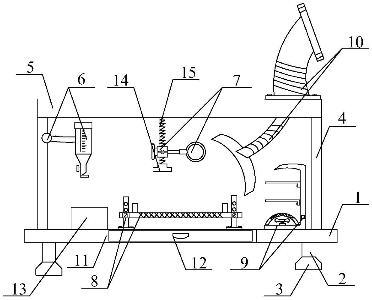
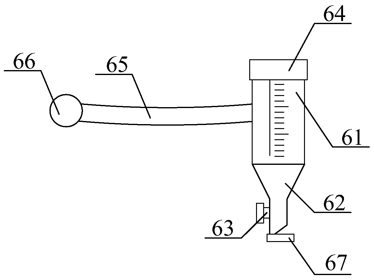
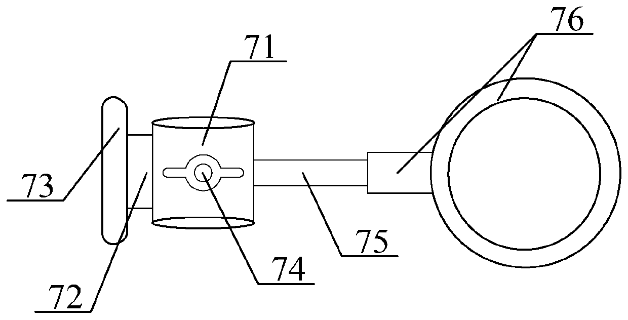
[0040] as attached figure 1 to attach figure 2 As shown, the present invention provides a multifunctional printed circuit board processing device, including a support base plate 1, a support screw lever 2, a rubber plate 3, a support column 4, a protective top plate 5, an adjustable solder paste storage bottle structure 6, Easy to wipe adjustable magnifying glass structure 7, adjustable circuit board processing support mesh structure 8, layered cooling shelf structure 9, smoke absorption connection tube structure for easy connection 10, drawer groove 11, drawer plate 12, welding seat 13. Limiting blocking cap 14 and screw column 15, the support screw levers 2 are respectively screwed to the four corners of the lower surface of the support base plate 1; the rubber disc 3 is screwed to the lower end of the support screw lever 2; The lower ends of the support columns 4 are respectively bolted to the four corners of the upper surface of the support base plate 1, and the upper en...


PUM


Abstract

The invention provides a multifunctional processing device for a printed circuit board. The device comprises a supporting base plate, a support screw lever, a rubber disc, a support column, a protective top plate, an adjustable solder paste storage bottle structure, a convenient-to-wipe adjustable magnifying lens structure, an adjustable circuit board processing support screen plate structure, a layered cooling placement frame structure, a convenient-to-connect flue gas absorption connection cylinder structure, a drawer groove, a drawer plate, a welding seat, a limiting stop cap and a screw rod column. Due to the arrangement of the solder paste storage bottle, a solder paste guide hopper, a manual control ball valve, a dustproof cover, a stainless steel flexible pipe, a rotary universal ball and a solder paste buffer box, the solder paste can be conveniently taken during the welding of a printed circuit board. Therefore, the use convenience is improved. Due to the arrangement of an adjusting sleeve, a magnet block, a wiping sponge pad, an adjusting screw and a welding magnifying lens, the magnifying welding operation is facilitated when small parts are welded on the printed circuitboard. Therefore, the wiping sponge pad can be used for wiping the lens welded with the magnifying lens.

Description

technical field [0001] The invention belongs to the technical field of printed circuit board processing, and in particular relates to a multifunctional printed circuit board processing device. Background technique [0002] Printed circuit boards, also known as printed circuit boards, are providers of electrical connections for electronic components. Its design is mainly layout design; the main advantage of using circuit boards is that it greatly reduces wiring and assembly errors, and improves the automation level and production labor rate. According to the number of layers of circuit boards, it can be divided into single-sided boards, double-sided boards, four-layer boards, six-layer boards and other multi-layer circuit boards. Since the printed circuit board is not a general terminal product, the definition of the name is slightly confusing. They are not the same, so when evaluating the industry, the two are related but cannot be said to be the same. Another example: be...

Claims


Application Information

Patent Timeline
IPC IPC(8): H05K3/34B23K3/00B23K3/06B23K3/08B08B1/00B08B15/02
Inventor 仲诺丁会李陆林杰虎
Owner 江西中信华电子工业有限公司
Why Eureka
Try Eureka