

An organic electroluminescent device
An electroluminescent device and luminescent technology, which is applied in the direction of organic semiconductor devices, electric solid devices, luminescent materials, etc., can solve problems that affect the luminous efficiency of organic electroluminescent devices and cannot guarantee the carrier transport capacity of the transport layer , to achieve low cost of use, reduce total reflection, and improve coupling efficiency
- Summary
- Abstract
- Description
- Claims
- Application Information
AI Technical Summary
Problems solved by technology
Method used
Image

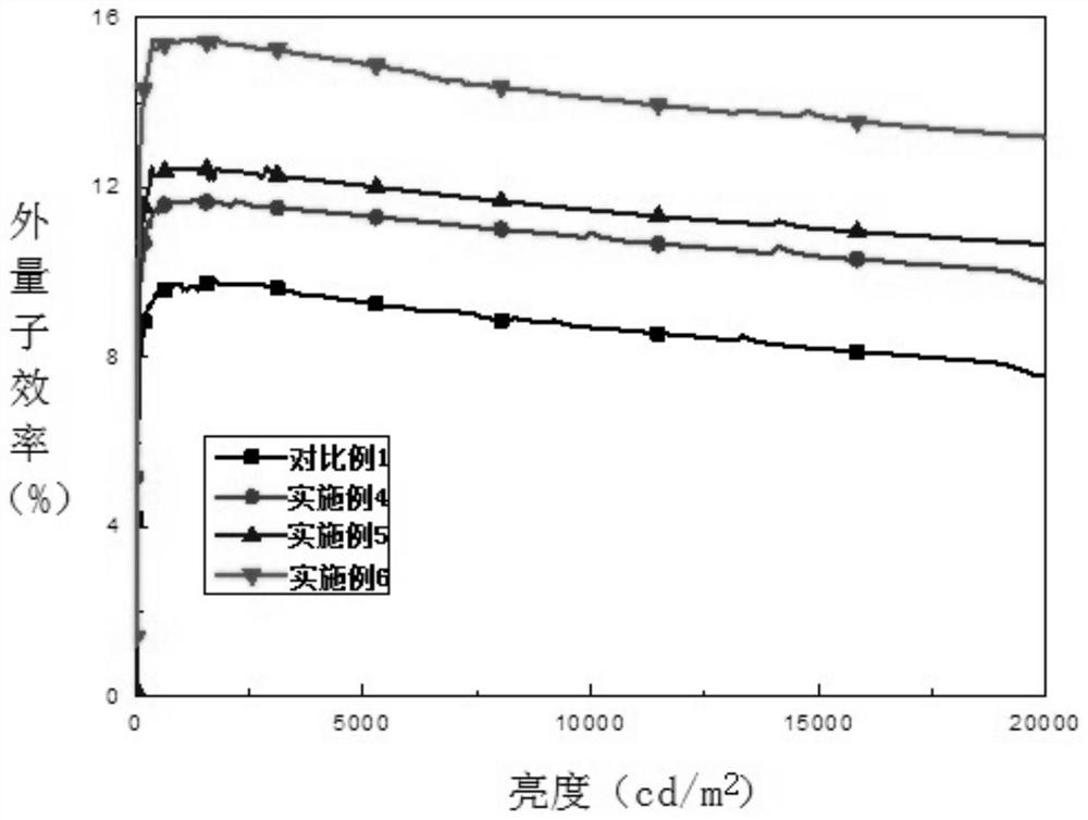
Examples
Embodiment 1
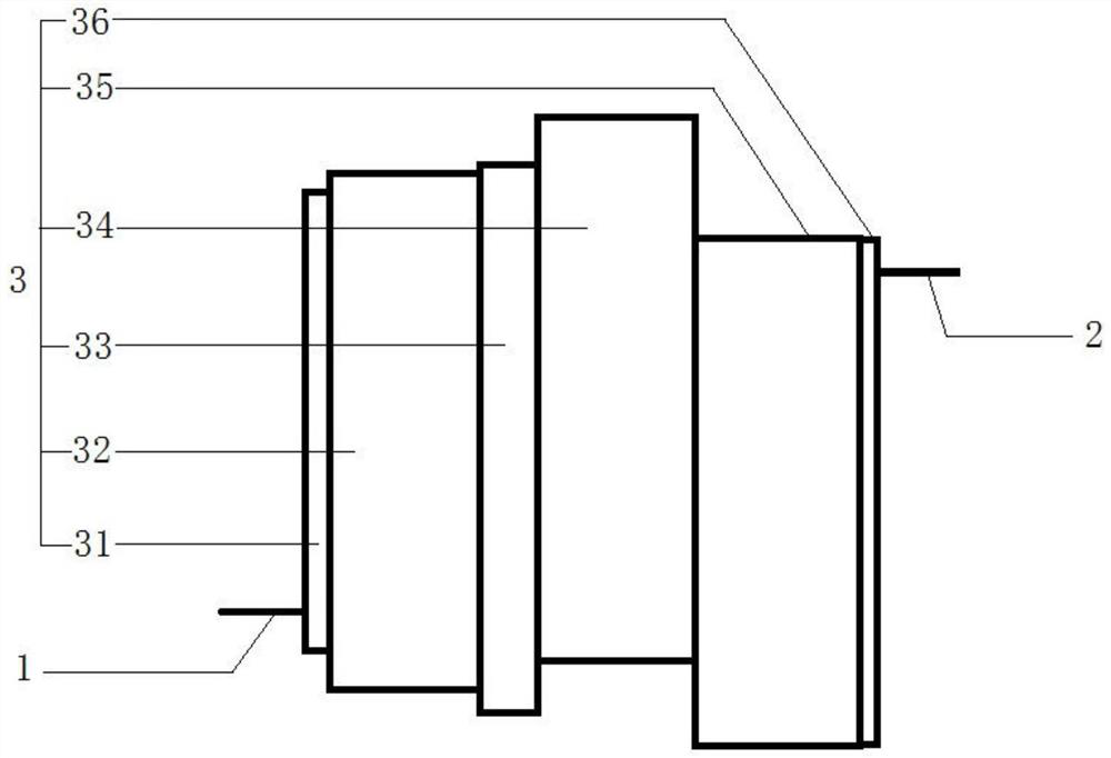
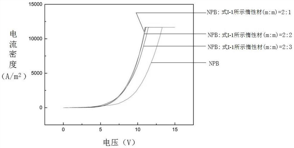
[0051] The invention provides an organic electroluminescence device, comprising a carrier transport layer, the carrier transport layer is a hole transport layer, including a hole transport material and an inert material doped in the hole transport material, The doping ratio of the inert material is 30wt%.
[0052] The structure of the inert material is as shown in formula I-1, n is 26, and the refractive index is 1.35.
[0053]
[0054] The hole transport material is N,N'-di(1-naphthyl)-N,N'-diphenyl-1,1'-biphenyl-4,4'-diamine (abbreviation: NPB). The molecular structure is shown in formula III-1:
[0055]
[0056] The preparation method of the carrier transport layer is as follows: the above-mentioned NPB and the inert material shown in the formula I-1 are subjected to vacuum doping evaporation at a mass ratio of 7:3 to form the carrier transport layer. Wherein, the evaporation condition of the inert material shown in formula I-1 is: 5*10 - 4 Under Pa vacuum degree,...
Embodiment 2
[0059] The invention provides an organic electroluminescent device, comprising a carrier transport layer, the carrier transport layer is an electron transport layer, including an electron transport material and an inert material doped in the electron transport material, the inert material The doping ratio was 20 wt%.
[0060] The selected inert material has a structure as shown in formula I-2, n is 10, and the refractive index is 1.3.
[0061]
[0062] The electron transport material is 4,7-diphenyl-1,10-phenanthroline (abbreviation: Bphen), and its molecular structure is shown in formula II-1:
[0063]
[0064] The preparation method of the carrier transport layer is as follows: the above-mentioned Bphen and the inert material shown in the formula I-2 are subjected to vacuum doping evaporation at a mass ratio of 8:2 to form the carrier transport layer. Among them, the inert material evaporation conditions shown in I-2 are: at 5*10 -4 Under Pa vacuum degree, the evapor...
Embodiment 3
[0067] The invention provides an organic electroluminescence device, comprising a carrier transport layer, the carrier transport layer is a hole transport layer, including a hole transport material and an inert material doped in the hole transport material, The doping ratio of the inert material is 60wt%.
[0068] The structure of the inert material is as shown in formula I-3, n is 30, and the refractive index is 1.36.
[0069]
[0070] The hole transport material is 4,4'-cyclohexylbis[N,N-bis(4-methylphenyl)]aniline (abbreviation: TAPC), and its molecular structure is shown in formula III-3:
[0071]
[0072] The preparation method of the carrier transport layer is as follows: the above-mentioned TAPC and the inert material shown in the formula I-3 are subjected to vacuum doping evaporation at a mass ratio of 4:6 to form the carrier transport layer. Wherein, the evaporation condition of the inert material shown in formula I-3 is: at 5*10 -4 Under Pa vacuum degree, the...
PUM
| Property | Measurement | Unit |
|---|---|---|
| Thickness | aaaaa | aaaaa |
| Thickness | aaaaa | aaaaa |
| Thickness | aaaaa | aaaaa |
Abstract
Description
Claims
Application Information