Processing method for calculating aliasing phenomenon in photoetching system model

A system model and computational lithography technology, applied in computing, computer components, pattern recognition in signals, etc., can solve problems such as distortion of light intensity calculations, reduction of accuracy of computational lithography models, etc.

Active Publication Date: 2019-07-05
MOYAN COMPUTATIONAL SCI NANJING PTE LTD
View PDF3 Cites 0 Cited by
  • Summary
  • Abstract
  • Description
  • Claims
  • Application Information

AI Technical Summary

Problems solved by technology

[0005] This application provides a processing method for calculating the aliasing phenomenon in the lithography system model, which can be used to solve the problem of freq...

Method used


Image

  • Processing method for calculating aliasing phenomenon in photoetching system model
  • Processing method for calculating aliasing phenomenon in photoetching system model
  • Processing method for calculating aliasing phenomenon in photoetching system model

Examples


Embodiment Construction

[0062] In order to enable those skilled in the art to better understand the technical solutions in the embodiments of the present application, and to make the above-mentioned purposes, features and advantages of the embodiments of the present application more obvious and understandable, the technical solutions in the embodiments of the present application are described below in conjunction with the accompanying drawings The program is described in further detail.

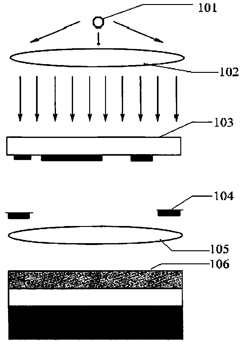
[0063] In the method provided in the embodiment of the present application, the execution subject of each step may be a terminal. The terminal is used to calculate the relevant data of the lithography system in the lithography process, and perform lithography according to the lithography model. Such as figure 1 mentioned. It shows a schematic diagram of the structure of the photolithography model. A light source 101 , a condenser lens 102 , a reticle 103 , a projection pupil 104 , a projection lens 105 and a wafe...


PUM


Abstract

The invention discloses a processing method for calculating an aliasing phenomenon in a photoetching system model, and the method comprises the steps of determining the number of sampling points for discrete sampling of a mask function according to an effective sampling range and a preset space sampling interval, wherein the mask function is used for representing the geometric shape of a mask; establishing an anti-aliasing filtering function according to the space sampling interval, wherein the anti-aliasing filtering function is used for limiting the bandwidth of the mask function in the frequency domain space; according to the anti-aliasing filtering function and the number of sampling points, carrying out the convolution operation for the anti-aliasing filtering function and the mask function, and obtaining the space sampling signals after the filtering of the mask function; and performing convolution operation on the space sampling signal and the kernel function to determine the light intensity distribution. In the application, the bandwidth of the mask function is limited by performing filtering sampling on the mask function through the anti-aliasing filter function, so that the light intensity calculation distortion caused by an aliasing phenomenon is avoided, and the accuracy of calculating the photoetching model can be improved.

Description

technical field [0001] The present application belongs to the technical field of semiconductor lithography, and in particular relates to a method for processing aliasing phenomena in computational lithography system models. Background technique [0002] Smart devices are inseparable from today's life, and smart phones, smart homes and smart wearable devices are generally related to everyone. The operation of smart devices is more of the silent operation of the chip behind the scenes. At present, in the production process of chips, the lithography technology, which is the key technology in chip production, uses the principle of photochemical reaction to transfer the pattern designed in advance on the mask to a wafer substrate, so that etching and ion implantation become possible. Diffraction occurs when light is irradiated on the mask, and the light of different diffraction orders converges on the surface of the photoresist. This process is an optical process; the image on ...

Claims


Application Information

Patent Timeline
IPC IPC(8): G06K9/00G06F17/15G06F17/14
CPCG06F17/14G06F17/15G06F2218/10G06F2218/02
Inventor 阎江崔绍春陈雪莲梁文清
Owner MOYAN COMPUTATIONAL SCI NANJING PTE LTD
Why Eureka
Try Eureka