TSV (Through-Silicon-Via) packaging structure and preparation method thereof

A packaging structure and enhanced structure technology, which is applied in semiconductor/solid-state device manufacturing, electrical components, electric solid-state devices, etc., can solve problems such as incomplete guarantee of structural strength and warpage, and achieve reduced TSV cost, low CTE, high intensity effect

Active Publication Date: 2019-07-09
JCET GROUP CO LTD
View PDF3 Cites 0 Cited by
  • Summary
  • Abstract
  • Description
  • Claims
  • Application Information

AI Technical Summary

Problems solved by technology

[0003] In the existing technology, due to the technical and cost challenges of TSV, in order to realize narrow-pitch interconnection, TSV holes with high aspect ratio are limited by equipment and process, and it is necessary to thin the chip or interposer to a thickness below 150 microns ; If so designed, it will bring huge challenges to subsequent processes such as holding and assembling
At the same time, in order to ensure the structural strength, it is necessary to carry out plastic sealing on the back and side, but due to the limitation of the strength of the plastic sealing compound, only the plastic sealing on the back and side cannot completely guarantee the overall structural strength
In addition, due to the CTE (coefficient of thermal expansion) mismatch between the mold compound and the chip, it will cause warpage problems

Method used


Image

  • TSV (Through-Silicon-Via) packaging structure and preparation method thereof
  • TSV (Through-Silicon-Via) packaging structure and preparation method thereof
  • TSV (Through-Silicon-Via) packaging structure and preparation method thereof

Examples


specific Embodiment

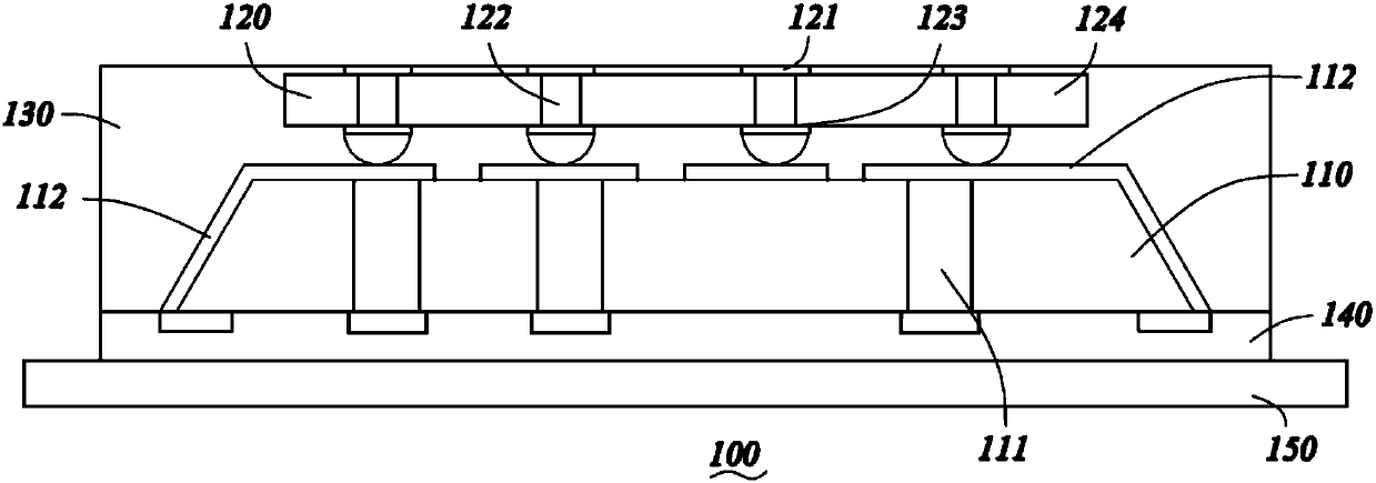
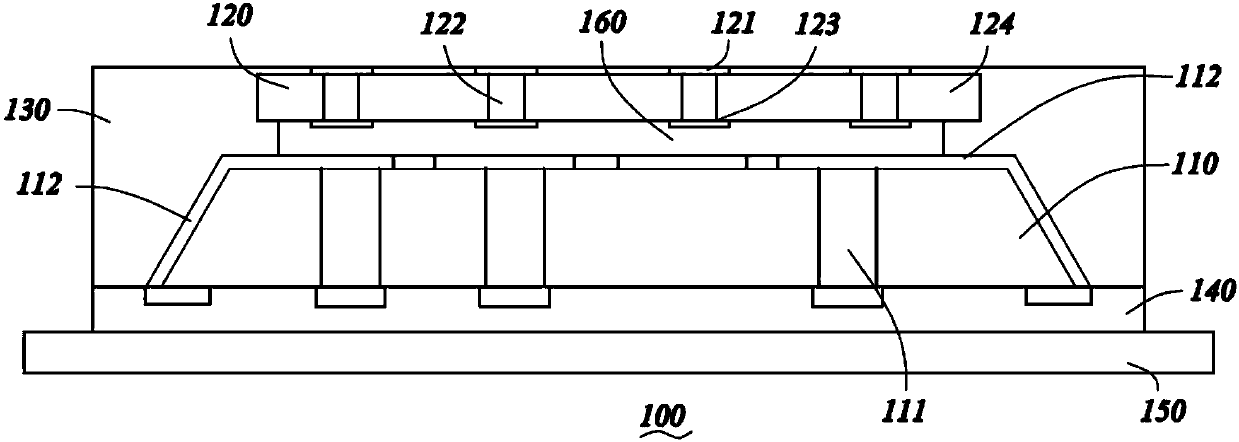
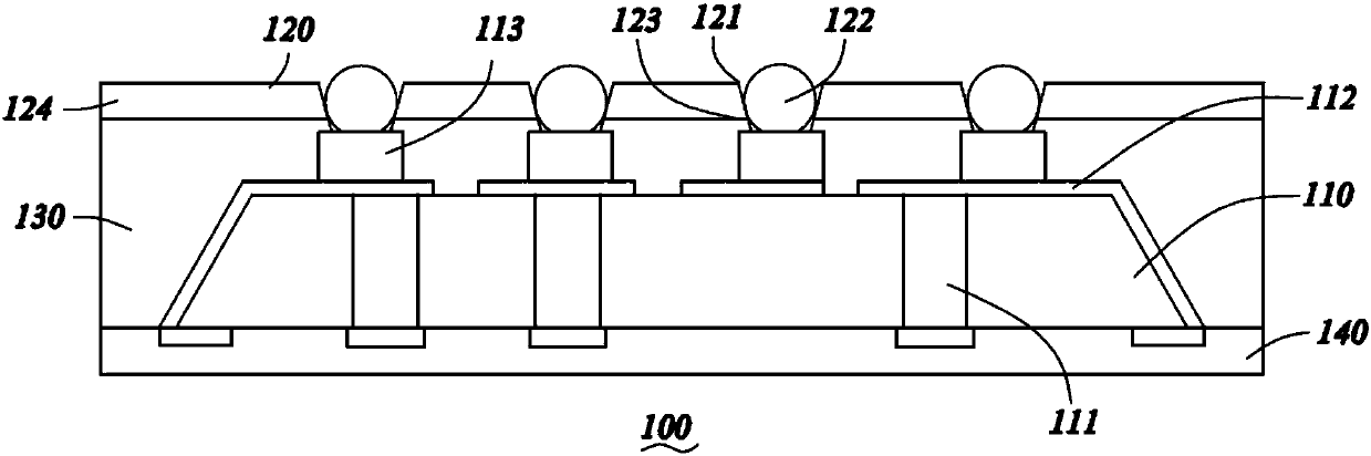
[0038] ginseng figure 1 As shown, the present invention proposes a TSV packaging structure 100. The TSV packaging structure 100 includes a TSV wafer 110. At the same time, the TSV wafer 110 includes a number of first through holes 111 etched through. The inner walls of the first through holes 111 are coated with There is conductive material to make the front and back of the TSV wafer 110 electrically connected. In this embodiment, the first through holes 111 are arranged vertically.

[0039] Further, connecting lines 112 are selectively laid on the back and side of the TSV wafer 110 to realize the connection between circuits disposed on the back and side of the TSV wafer 110 .

[0040] Further, the TSV package structure 100 also includes a reinforcement structure 120 assembled to the back of the TSV wafer and electrically connected to the connection line 112. Specifically, the assembly method proposed in the present invention includes flip-chip or front-mount, and the common p...


PUM


Abstract

The invention discloses a TSV (Through-Silicon-Via) packaging structure. The TSV packaging structure comprises a TSV wafer and a reinforcement structure, wherein the TSV wafer comprises a plurality offirst vias etched in a run-through mode; the inner walls of the first vias are coated with conducting materials so as to electrically conduct the front side and the reverse side of the TSV wafer; connection lines are selectively laid at the reverse side and on the lateral surface of the TSV wafer; the reinforcement structure is assembled to the reverse side of the TSV wafer; the reinforcement structure comprises first electrical connection ends facing away from the reserve side of the TSV wafer and second electrical connection ends abutted and electrically conducted with the connection lines;and the first electrical connection ends and the second electrical connection ends are electrically conducted. According to the TSV packaging structure disclosed by the invention, by assembling the reinforcement structure to the TSV wafer, when low CTE (Coefficient of Thermal Expansion), high intensity and a high modulus are ensured, high intensity and low warping of packaging are also ensured. Meanwhile, a preparation method of the TSV packaging structure, which is disclosed by the invention, can simultaneously meet requirements for reducing TSV cost and ensuring packaging intensity and warping.

Description

technical field [0001] The invention belongs to the field of semiconductor manufacturing, and in particular relates to a TSV packaging structure and a preparation method thereof. Background technique [0002] TSV (Through-Silicon-Via) is formed by etching a vertical through-hole or a through-hole and through-hole through the substrate and filling the through-hole with a conductive material such as copper, or forming a conductive circuit on the sidewall of the through-hole . The TSVs may be used to provide electrical connection from the backside of the semiconductor substrate to semiconductor circuitry on the opposite side of the substrate, or to semiconductor circuitry of stacked die. [0003] In the existing technology, due to the technical and cost challenges of TSV, in order to realize narrow-pitch interconnection, TSV holes with high aspect ratio are limited by equipment and process, and it is necessary to thin the chip or interposer to a thickness below 150 microns ; ...

Claims


Application Information

Patent Timeline
Patent Type & Authority Applications(China)
IPC IPC(8): H01L21/768H01L23/31H01L23/48
CPCH01L21/76898H01L23/31H01L23/481H01L2225/06541H01L2224/16H01L2924/181H01L2924/18161H01L2924/00012
Inventor 林耀剑
Owner JCET GROUP CO LTD
Why Eureka
Try Eureka